Amplification device with a bias circuit

a bias circuit and amplifier technology, applied in the field of amplifiers, can solve the problems of inability to realistically embed the resistance element of such a huge size, the esd tolerance is too high, and the bias voltage is highly stable, so as to improve the high reliability and high esd tolerance.

Inactive Publication Date: 2006-10-10
COLLABO INNOVATIONS INC
View PDF3 Cites 12 Cited by
  • Summary
  • Abstract
  • Description
  • Claims
  • Application Information

AI Technical Summary

Benefits of technology

[0010]An object of the present invention is to provide an amplification device wherein the whole of a bias circuit and an amplifier circuit is embedded on the same substrate with any of an extremely high input impedance, a high ESD tolerance, and a highly stable bias voltage maintained, thereby achieving the compatibility between further higher integration and further improvement in high reliability.
[0030]The above-described MOSFET according to the invention also has a function of protecting the amplifier circuit from ESD as follows. When a surge voltage caused by ESD is applied from the surroundings to the input terminal of the amplifier circuit, the above-described MOSFET is brought into conduction between the drain and the source, thereby connecting the input terminal of the amplifier circuit to the high or low side power supply terminal. Here, the conduction is established by one of the following: a breakdown at a diode (PN junction) parasitic between the drain or source and the backgate; a turn-on of a bipolar transistor parasitic among the drain, the source, and the backgate; and the channel generation between the drain and the source. Because of the drain-source conduction, the surge energy is absorbed into the power supply or the ground conductor. Thus, adverse effects of the surge on the amplifier circuit and the following stages are avoided. In other words, the above-described amplification device according to the invention is resistant to ESD.
[0031]In the above-described MOSFET according to the invention, no leak current flows through the input terminal of the amplifier circuit since it has the MOSFET input stage. Accordingly, the drain- or source-backgate PN junction included in the above-described MOSFET is not reverse-biased by the leak current of the amplifier circuit. In the other words, the potential of the input terminal of the amplifier circuit is stably maintained equal to the bias voltage. The bias voltage is stable enough, in particular, even if the above-described PN junctions are provided with reduced areas in order to miniaturization, thereby being provided with higher resistances to reverse bias and further exhibiting a wide range of the resistance variations. Thus, the above-described bias circuit according to the invention maintains both of the high reliability of its ESD protection and the high stability of the bias voltage.
[0032]In the amplification device according to the invention, the bias circuit achieves a sufficiently high output impedance, using the above-described MOSFET, as described above. Thereby, the whole of the bias circuit and the amplifier circuit is embedded on the same substrate with the extremely high input impedance, the high ESD tolerance, and the highly stable bias voltage maintained. As a result, the above-described amplification device according to the invention achieves the compatibility between further higher integration and further improvement in high reliability. The above-described amplification device according to the invention is superior especially to other amplification devices connected directly to low-frequency signal sources with high internal impedances such as vibration sensors.

Problems solved by technology

There is an upper limit for sheet resistances, which is usually of a few tens of kilo ohms, due to a limit of control over impurity concentration.
Embedded resistance element of such a huge size would not be realistic.
Therefore, for the conventional amplification device 100, miniaturization by further higher integration is difficult.
Integrated circuits are susceptible to adverse influences of the surrounding electrostatic discharge (ESD) through terminals connected to the outside.
However, a minute leak current flows in the reverse-biased PN junction.
Such an excessive variation of the bias voltage is undesirable since it can interfere with the operation of the amplification device 100, and further, it can cause the potential of the output terminal OUT of the amplification device 100, that is, the bias voltage for the next-stage amplification device to vary excessively.
Accordingly, severe restrictions can be imposed on the design of the following amplification devices.
Therefore, it is difficult to further improve the reliability of the whole of the multistage amplification device.

Method used


Image

  • Amplification device with a bias circuit
  • Amplification device with a bias circuit
  • Amplification device with a bias circuit

Examples


embodiment 1

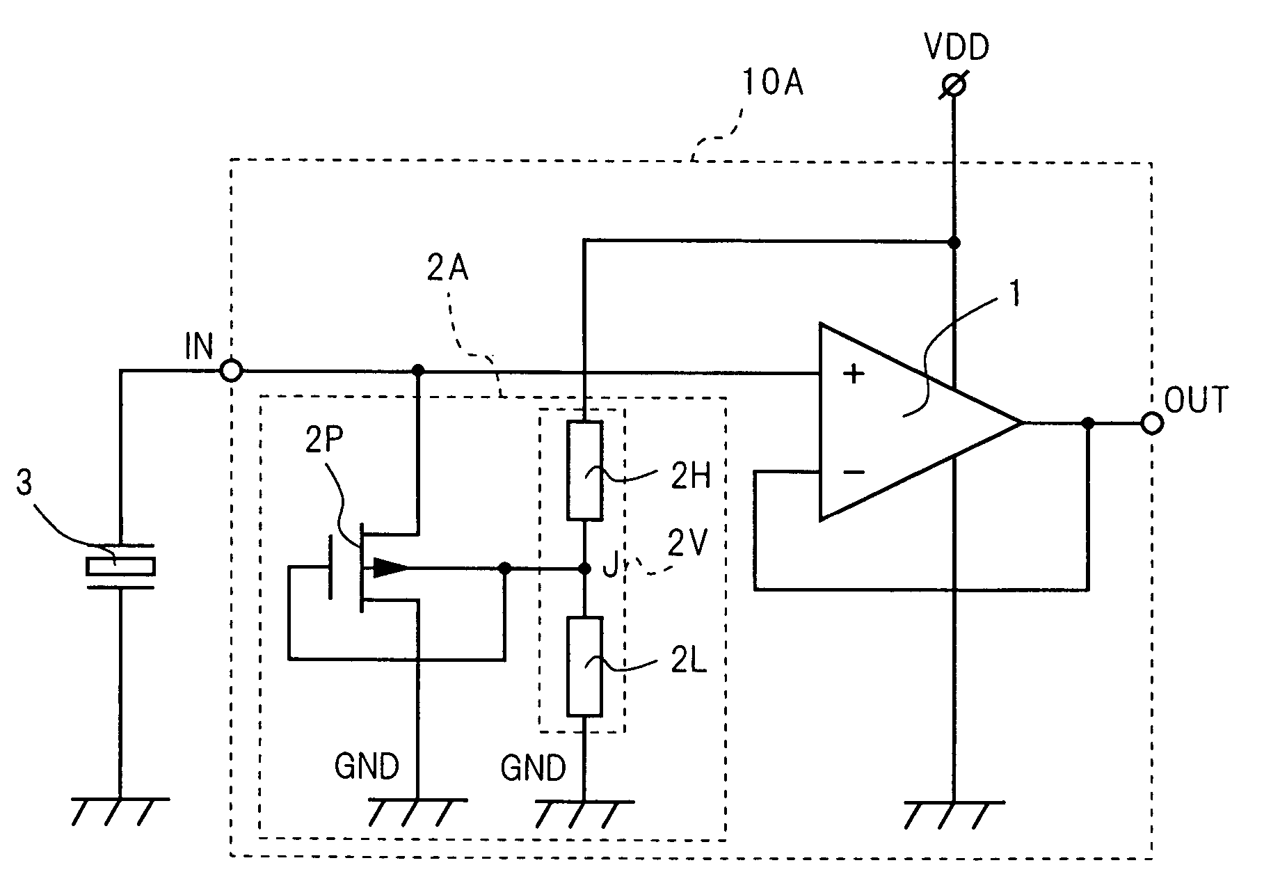
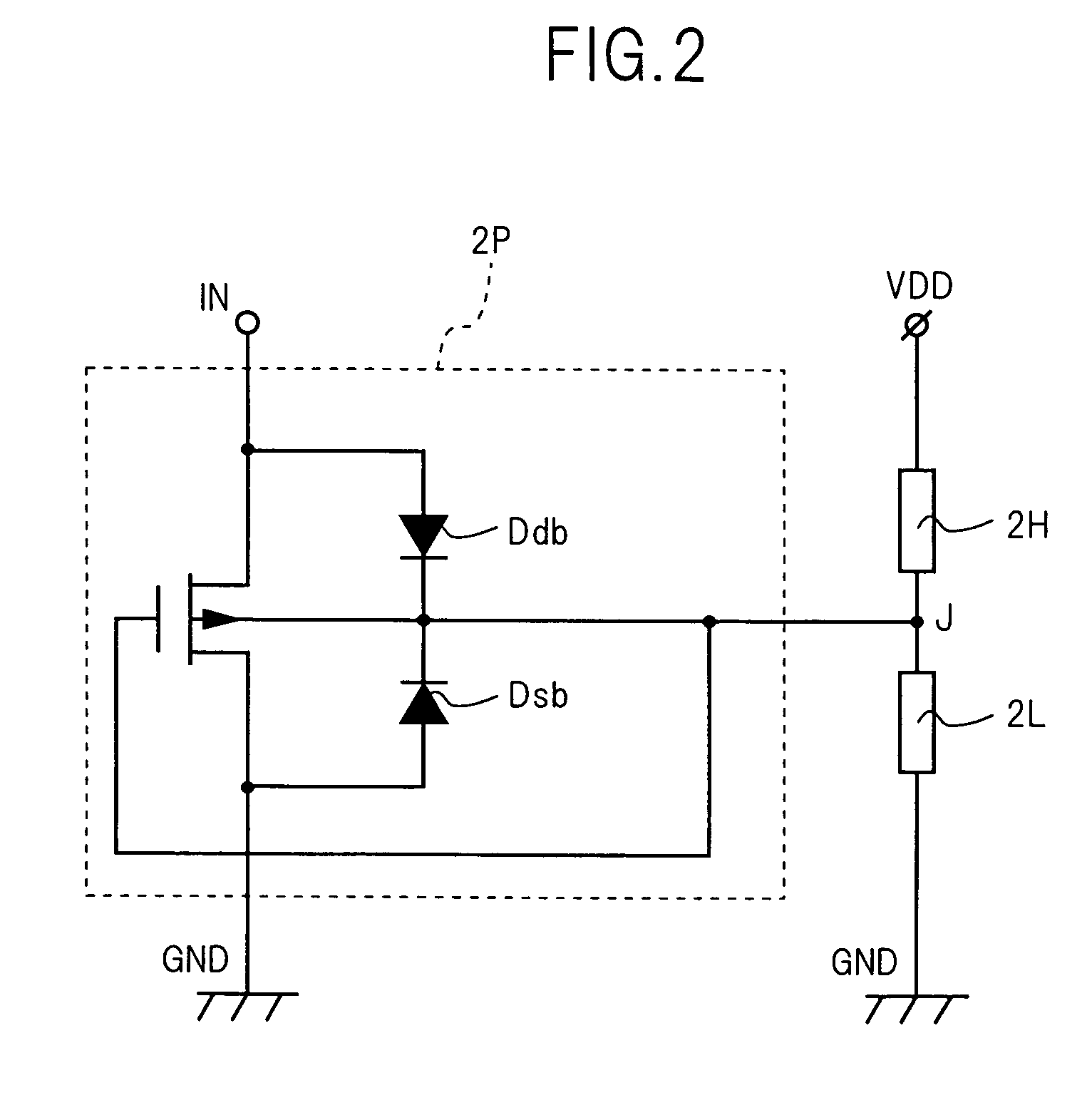
[0044]An amplification device according to Embodiment 1 of the invention is preferably used for the first stage of a multistage amplification device. The amplification device amplifies signals provided from, for example, a miniature vibration sensor. The vibration sensor is preferably of a piezoelectric type, which uses a piezoelectric device. The vibration sensor may alternatively be an ECM. An amplification device 10A according to Embodiment 1 of the invention is connected directly to a piezoelectric device 3. See FIG.1. This amplification device 10A is preferably a single integrated circuit, which is embedded on a single substrate. The amplification device 10A comprises a high side power supply terminal VDD, a low side power supply terminal GND, an operational amplifier 1, and a bias circuit 2A. The bias circuit 2A includes a bias voltage generating section 2V and an impedance element 2P.

[0045]The high side power supply terminal VDD is connected to an external constant-voltage so...

embodiment 2

[0053]The amplification device 10B according to Embodiment 2 of the invention is connected directly to the piezoelectric device 3, similarly to the amplification device 10A according to Embodiment 1. See FIG. 3. This amplification device 10B is preferably a single integrated circuit, which is embedded on a single substrate. The amplification device 10B comprises a configuration in common with the amplification device 10A according to Embodiment 1, except for the configuration of a bias circuit 2B. In FIG. 3, the components similar to the components shown in FIG. 1 are marked with the same reference symbols as the reference symbols shown in FIG. 1. Furthermore, for the details of the similar components, the explanation about Embodiment 1 is cited.

[0054]The bias circuit 2B includes a p-channel MOSFET 2Q for use as an impedance element, similarly to the bias circuit 2A according to Embodiment 1. However, the gate of the p-channel MOSFET 2Q is connected to the drain, in contrast to the ...

embodiment 3

[0058]The amplification device 10C according to Embodiment 3 of the invention is connected directly to the piezoelectric device 3, similarly to the amplification device 10A according to Embodiment 1. See FIG. 4. This amplification device 10C is preferably a single integrated circuit, which is embedded on a single substrate. The amplification device 10C comprises a configuration in common with the amplification device 10A according to Embodiment 1, except for the configuration of a bias circuit 2C. In FIG. 4, the components similar to the components shown in FIG. 1 are marked with the same reference symbols as the reference symbols shown in FIG. 1. Furthermore, for the details of the similar components, the explanation about Embodiment 1 is cited.

[0059]The bias circuit 2C includes an n-channel MOSFET 2N for use as an impedance element, instead of the p-channel MOSFET 2P, in contrast to the bias circuit 2A according to Embodiment 1. The n-channel MOSFET 2N is of an enhancement type. T...


PUM


Abstract

An operational amplifier amplifies a signal received through its input terminal connected directly to a piezoelectric device. A bias voltage generating section includes a voltage divider between the power supply terminal and the ground terminal. The drain and source of a p-channel MOSFET are connected to the input terminal of the operational amplifier and the ground terminal. Since the voltage divider applies a bias voltage to the gate and the backgate, the p-channel MOSFET maintains the OFF state. Since a drain-backgate parasitic diode clamps the drain potential to the bias voltage, the bias voltage is applied to the input terminal of the operational amplifier. Then, the drain-backgate resistance is extremely high. The p-channel MOSFET is embedded on a substrate together with other circuits of the amplification device. Thus, the amplification device with an extremely high input impedance is configured as a single integrated circuit.

Description

BACKGROUND OF THE INVENTION[0001]This invention relates to amplification devices, in particular, amplification devices connected to signal sources with high internal impedances.[0002]Vibration sensors are sensors for detecting forces exerted on an object to be measured, in other words, for detecting accelerations of the object, and for converting the magnitudes of the forces into electric signals. The range of uses of vibration sensors is wide, which include, for example: monitoring of abnormal vibration in motors etc.; control of a balance of lathe etc.; monitoring of conditions of air conditioners etc.; measurements of characteristics of HDDs etc.; medical diagnoses and treatments using ultrasonically vibration etc.; hand movement detection for digital video cameras etc.; and sound detection for cellular phones etc. In many of those uses, both of miniaturization and high reliability are demanded of vibration sensors.[0003]The vibration sensors of miniature size widely used in gene...

Claims


Application Information

Patent Timeline
Patent Type & Authority Patents(United States)
IPC IPC(8): H03F3/16H03F1/30H03F1/52H03F3/185H03F3/45
CPCH03F1/30H03F3/185H03F3/45475H03F2200/228
Inventor SATO, MASAHARU
Owner COLLABO INNOVATIONS INC
Why Eureka
Try Eureka