Controlled polymerization on plasma reactor wall

a plasma reactor and polymerization technology, applied in the field of semiconductor fabrication, can solve the problems of high aluminum level, other defects in the etched silicon, and generalized poor practice of dramatic change of plasma state during etching

Inactive Publication Date: 2006-10-17
APPLIED MATERIALS INC
View PDF13 Cites 26 Cited by
  • Summary
  • Abstract
  • Description
  • Claims
  • Application Information

AI Technical Summary

Problems solved by technology

It is generally considered poor practice to dramatically change the plasma state during an etching even if endpoint detection is made.
Interactions of the silicon etching plasma with the anodized aluminum wall are believed to be responsible for high aluminum levels and other defects in the etched silicon.

Method used


Image

  • Controlled polymerization on plasma reactor wall
  • Controlled polymerization on plasma reactor wall
  • Controlled polymerization on plasma reactor wall

Examples


Embodiment Construction

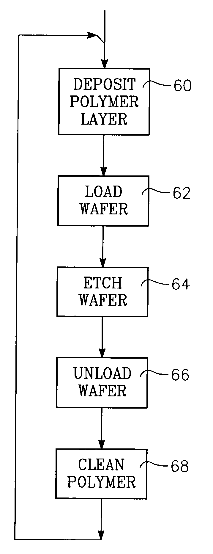
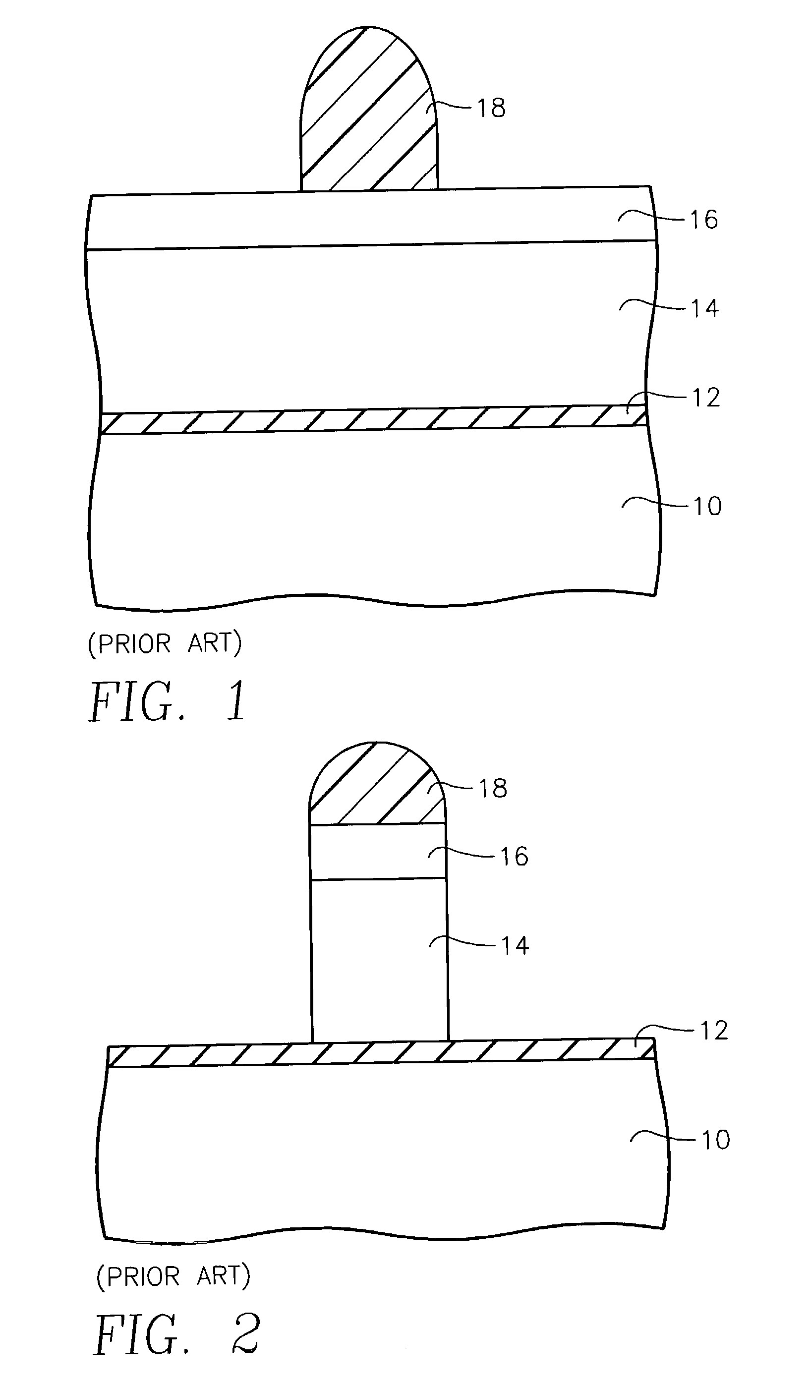
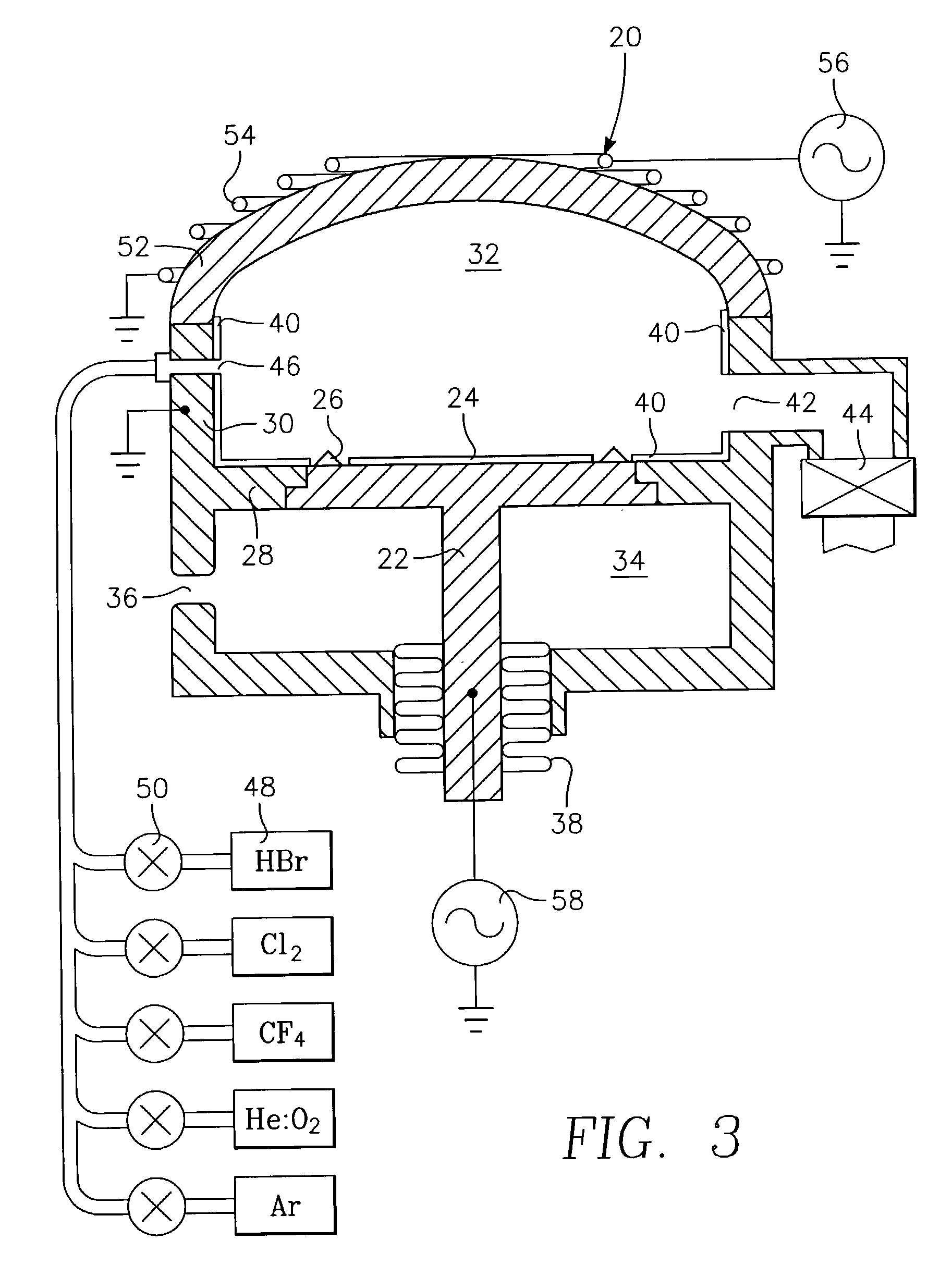
[0017]The variabilities described above in the breakthrough and main etches are believed to arise from relatively uncontrolled polymerization on the chamber sidewalls or its sidewall shields as the polymer is being deposited in the breakthrough etch but removed in the main etch. Whether a chamber sidewall or other chamber part is bare or covered by polymer will affect the plasma chemistry. For example, the presence of the carbonaceous polymer on the sidewall tends to scavenge oxygen from the main etch plasma while a bare chamber wall does not. The etch rate for the polysilicon main etch has been observed to change 10 to 20% when the chamber wall changes from being coated with polymer to being clean.

[0018]If there is more polymer deposited than is removed, that is, positive net polymer deposition, the polymer thickness builds up from one wafer to the next. Positive net polymerization is considered quite disadvantageous because the polymer thickness keeps building up until the polymer...


PUM

PropertyMeasurementUnit
thicknessaaaaaaaaaa
thickaaaaaaaaaa
timeaaaaaaaaaa

Abstract

An integrated etch process, for example as used for etching an anti-reflection layer and an underlying aluminum layer, in which the chamber wall polymerization is controlled by coating polymer onto the sidewall by a plasma deposition process prior to inserting the wafer into the chamber, etching the structure, and after removing the wafer from the chamber, plasma cleaning the polymer from the chamber wall. The process is process is particularly useful when the etching is performed in a multi-step process and the polymer is used for passivating the etched structure, for example, a sidewall in an etched structure and in which the first etching step deposits polymer and the second etching step removes polymer. The controlled polymerization eliminates interactions of the etching with the chamber wall material, produces repeatable results between wafers, and eliminates in the etching plasma instabilities associated with changing wall conditions.

Description

BACKGROUND OF THE INVENTION[0001]1. Field of the Invention[0002]The invention relates generally to semiconductor fabrication. In particular, the invention relates to plasma etching processes and chamber seasoning.[0003]2. Background Art[0004]The fabrication of modem semiconductor integrated circuits requires etching processes of carefully controlled chemistry and processing conditions in order to achieve anisotropic and selective etching of thin layers. One example involving silicon etching is illustrated in the cross-sectional view of FIG. 1. A silicon substrate 10 is covered with a thin gate oxide layer 12 having a composition of approximately SiO2 and a thickness of about 1 to 10 nm. A polysilicon layer 14 is deposited over the gate oxide layer 12. It is intended to act as a lateral conductor so it is relatively thick, for example, 120 nm or more. An anti-reflection coating (ARC) 16 is deposited over the polysilicon layer 14. Its thickness and dielectric constant are chosen to pr...

Claims


Application Information

Patent Timeline
Patent Type & Authority Patents(United States)
IPC IPC(8): B44C1/22H01J37/32H01L21/00H01L21/311H01L21/3213
CPCH01J37/32009H01J37/32532H01L21/31116H01L21/31138H01L21/32137H01L21/32139H01L21/67069
Inventor DESHMUKH, SHASHANK C.LILL, THORSTEN B.
Owner APPLIED MATERIALS INC
Why Eureka
Try Eureka