Method and apparatus for non-contact testing and diagnosing electrical paths through connectors on circuit assemblies

a technology of electrical paths and connectors, which is applied in short-circuit testing, resistance/reactance/impedence, instruments, etc., can solve problems such as “open” defects, interference with the success of capacitive lead-frame testing, and lack of capacitive coupling between an ic lead-frame and a tester's sense pla

Inactive Publication Date: 2006-10-17
AGILENT TECH INC
View PDF5 Cites 34 Cited by
  • Summary
  • Abstract
  • Description
  • Claims
  • Application Information

AI Technical Summary

Problems solved by technology

Note, however, that one of the leads 108 is not soldered to the printed circuit board, thereby resulting in an “open” defect.
If CSense is significantly larger than any possible CJoint, a bad lead will result in the AC detector seeing a capacitance near CJoint.
Over the years, various factors have interfered with the success of capacitive lead-frame testing.
One factor is a lack of capacitive coupling between an IC lead-frame and a tester's sense plate.
This problem is largely traced to the on-going miniaturization of IC packages and their lead-frames, as well as the imposition of ground shield and heat sinks between lead-frames and the sensor plate (some of which are internal to an IC's package).
They can also interfere with capacitive lead-frame testing in that they sometimes make it difficult to position the sense plate of a capacitive lead-frame tester in close enough proximity to their lead-frames.
They can also present a problem as they have a limited area for sensing purposes.
Another factor that has interfered with the success of capacitive lead-frame testing is the ratio of non-signal leads to total leads on an IC package.
Capacitive lead-frame testing is not designed to detect opens on such leads.
Thus, a significant fraction of IC leads could suffer from opens that cannot be tested.
Another factor that has interfered with the success of capacitive lead-frame testing is socket-mounted IC packages.
This adds a layer of complexity to testing in that proper connection between the board and package requires proper connection between the board and socket.
However, all of these techniques depend on the inserted device's inherent testability for opens coverage; and even if the inserted device is suited to application of these techniques, only signal leads will be adequately tested, and redundant power and ground connections will only be “grossly” tested.
If the inserted device has poor testability, neither the inserted device nor the socket will be adequately tested.
Also, sockets are easily damaged, so there are opportunities to damage a socket that must be minimized during manufacture, shipping, handling, attachment to the printed circuit board, testing or during insertion of the IC into the socket.
Yet another factor that has frustrated the success of capacitive lead frame testing is the addition of more and more connectors to printed circuit assemblies, such as edge connectors, motherboard connectors, daughter board connectors, etc.
These connectors have delicate connector pins that are easily bent or damaged during mating and when left open and unprotected.
Connectors are becoming denser and more complex., adding to the causes of printed circuit assembly failures during manufacturing, handling and test.
The amount of force required to mate these denser connectors is significant and can easily damage or destroy misaligned connector pins, the attachment point between the connector and the circuit assembly or the circuit assembly.
However, mating and de-mating of circuit assembly connectors is generally done manually, due to the forces involved and the potential for damage.

Method used


Image

  • Method and apparatus for non-contact testing and diagnosing electrical paths through connectors on circuit assemblies
  • Method and apparatus for non-contact testing and diagnosing electrical paths through connectors on circuit assemblies
  • Method and apparatus for non-contact testing and diagnosing electrical paths through connectors on circuit assemblies

Examples


Embodiment Construction

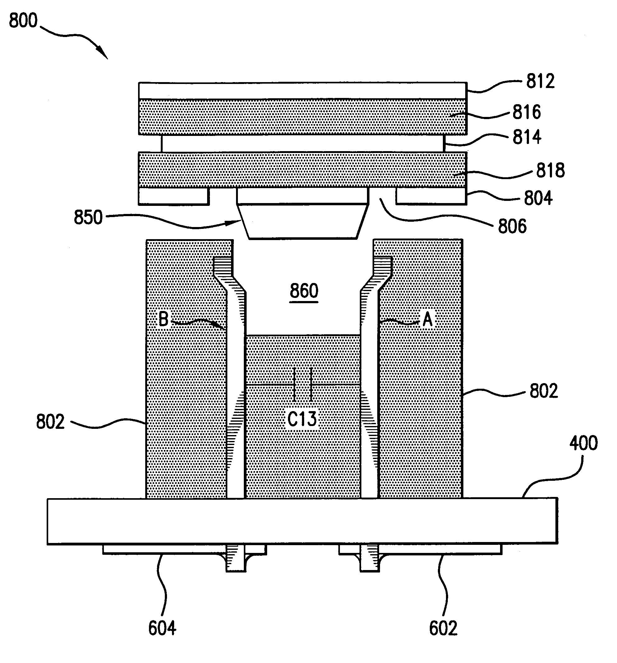
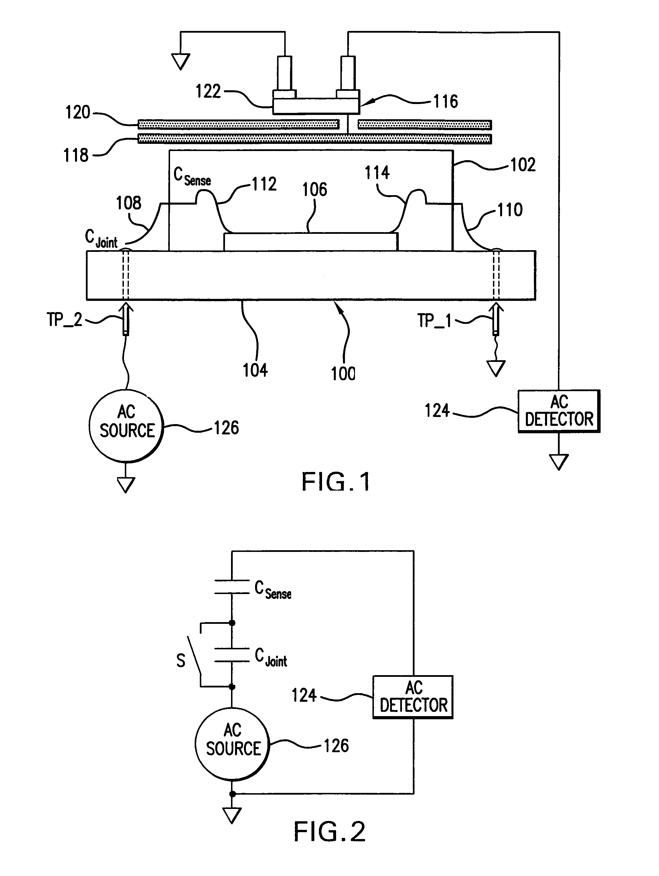
[0025]The United States patent application of Kenneth P. Parker, et al. entitled “Methods and Apparatus for Testing Continuity of Electrical Paths Through Connectors of Circuit Assemblies”, USPTO Ser. No. 10 / 683,693, filed Oct. 9, 2003, is hereby incorporated by reference and discloses how to determine whether defects exist in one or more of a plurality of electrical paths through sockets or other connectors.

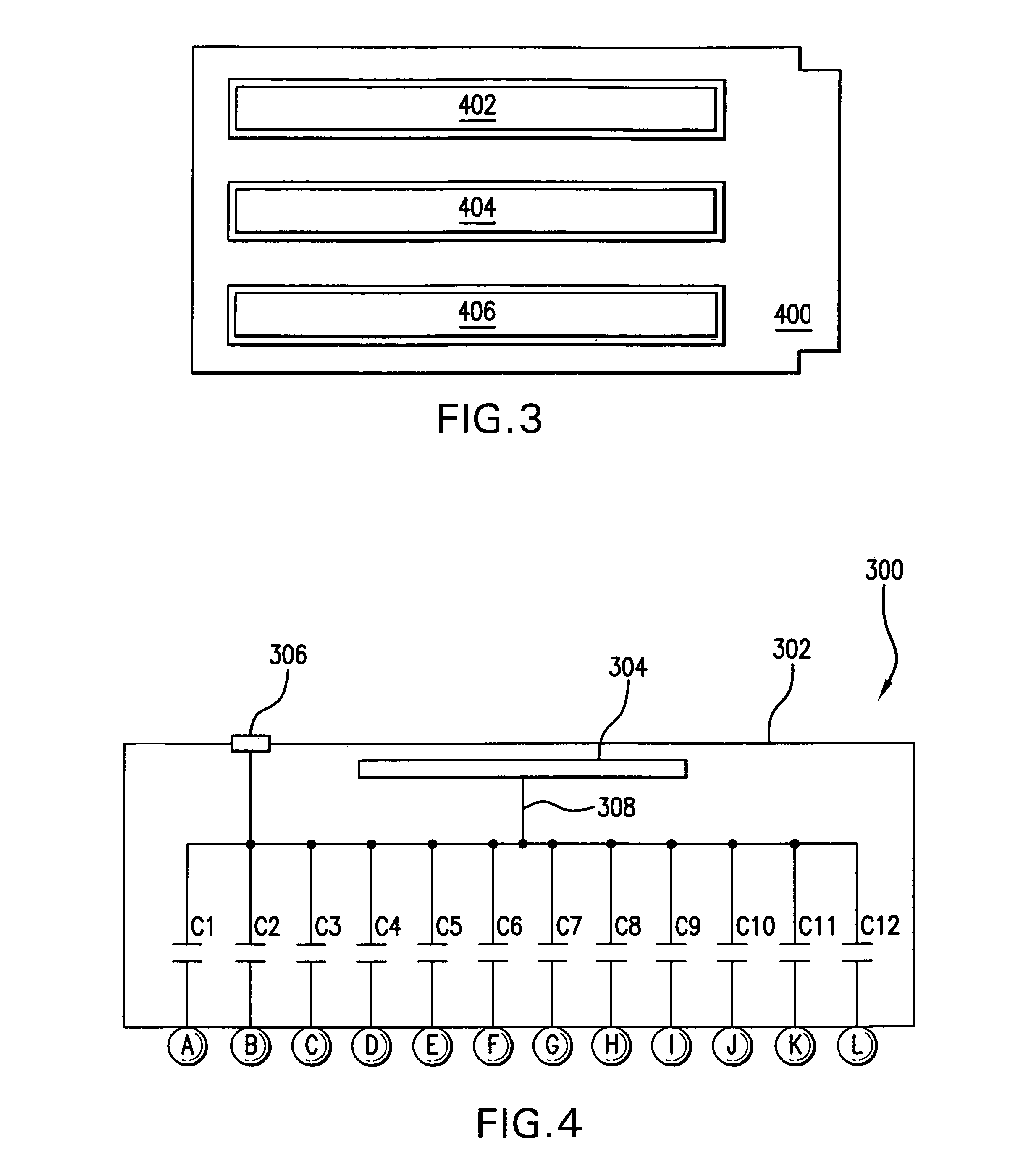
[0026]One exemplary apparatus disclosed in the afore-mentioned patent application is shown in FIGS. 3 and 4. FIG. 3 illustrates a circuit assembly 400 comprising connectors 402, 404, 406 for receiving random access (RAM) modules, mother boards, daughter board, memory cards, etc. FIG. 4 illustrates a first exemplary embodiment of a device 300 for testing continuity of electrical paths through connectors 402, 404 and 406 of a circuit assembly 400. By way of example, the device 300 is configured to test electrical paths of connectors 402, 404 and 406 on circuit assembly 400, shown ...


PUM


Abstract

A device for enabling testing of electrical paths through a circuit assembly is presented. The device may include a non-contact connector test probe for a testing a connector of the circuit assembly. A method for testing continuity of electrical paths through a circuit assembly is presented. In the method, one or more nodes of the circuit assembly are stimulated, connector pins of a connector on the circuit assembly are capacitively coupled to a non-contact connector test probe, and an electrical characteristic is measured by a tester coupled to the non-contact connector test probe to determine continuity of electrical paths through the circuit assembly.

Description

BACKGROUND OF THE INVENTION[0001]During manufacture, circuit assemblies (e.g., printed circuit boards and Multi-Chip Modules) need to be tested for interconnect defects such as open solder joints, broken connectors, and bent or misaligned leads (e.g., pins, balls, or spring contacts). One way to test for such defects is via capacitive lead-frame testing. FIGS. 1 & 2 illustrate an exemplary setup for capacitive lead-frame testing. FIG. 1 illustrates a circuit assembly 100 comprising an integrated circuit (IC) package 102 and a printed circuit board 104. Enclosed within the IC package is an IC 106. The IC is bonded to the leads 108, 110 of a lead-frame via a plurality of bond wires 112, 114. The leads, in tum, are meant to be soldered to conductive traces on the printed circuit board. Note, however, that one of the leads 108 is not soldered to the printed circuit board, thereby resulting in an “open” defect.[0002]Positioned above the IC package 102 is a capacitive lead-frame test asse...

Claims


Application Information

Patent Timeline
Patent Type & Authority Patents(United States)
IPC IPC(8): G01R31/02G01R27/26G01R31/04G01R31/312
CPCG01R31/026G01R31/312G01R31/046G01R31/70G01R31/54G01R31/52
Inventor PARKER, KENNETH P.JACOBSEN, CHRIS R.SCHNEIDER, MYRON J.
Owner AGILENT TECH INC
Why Eureka
Try Eureka