Differential amplification input circuit

a technology of input circuit and differential amplification, which is applied in the field of input circuit, can solve the problems that the amplification circuit b>20/b> is difficult to transfer the high frequency signal to the preamplifier circuit , the adjustment of large offsets cannot be made to narrow the voltage range of measuring signals, etc., and achieves high input impedance, increased input voltage range, and stable operation

a technology of input circuit and differential amplification, which is applied in the field of input circuit, can solve the problems that the amplification circuit b>20/b> is difficult to transfer the high frequency signal to the preamplifier circuit , the adjustment of large offsets cannot be made to narrow the voltage range of measuring signals, etc., and achieves high input impedance, increased input voltage range, and stable operation

US7123080B2Active Publication Date: 2006-10-17YOKOGAWA ELECTRIC CORP

Image

  • Differential amplification input circuit
  • Differential amplification input circuit
  • Differential amplification input circuit

Examples


Embodiment Construction

[0041]An embodiment of the present invention will be described below with reference to the accompanying drawings.

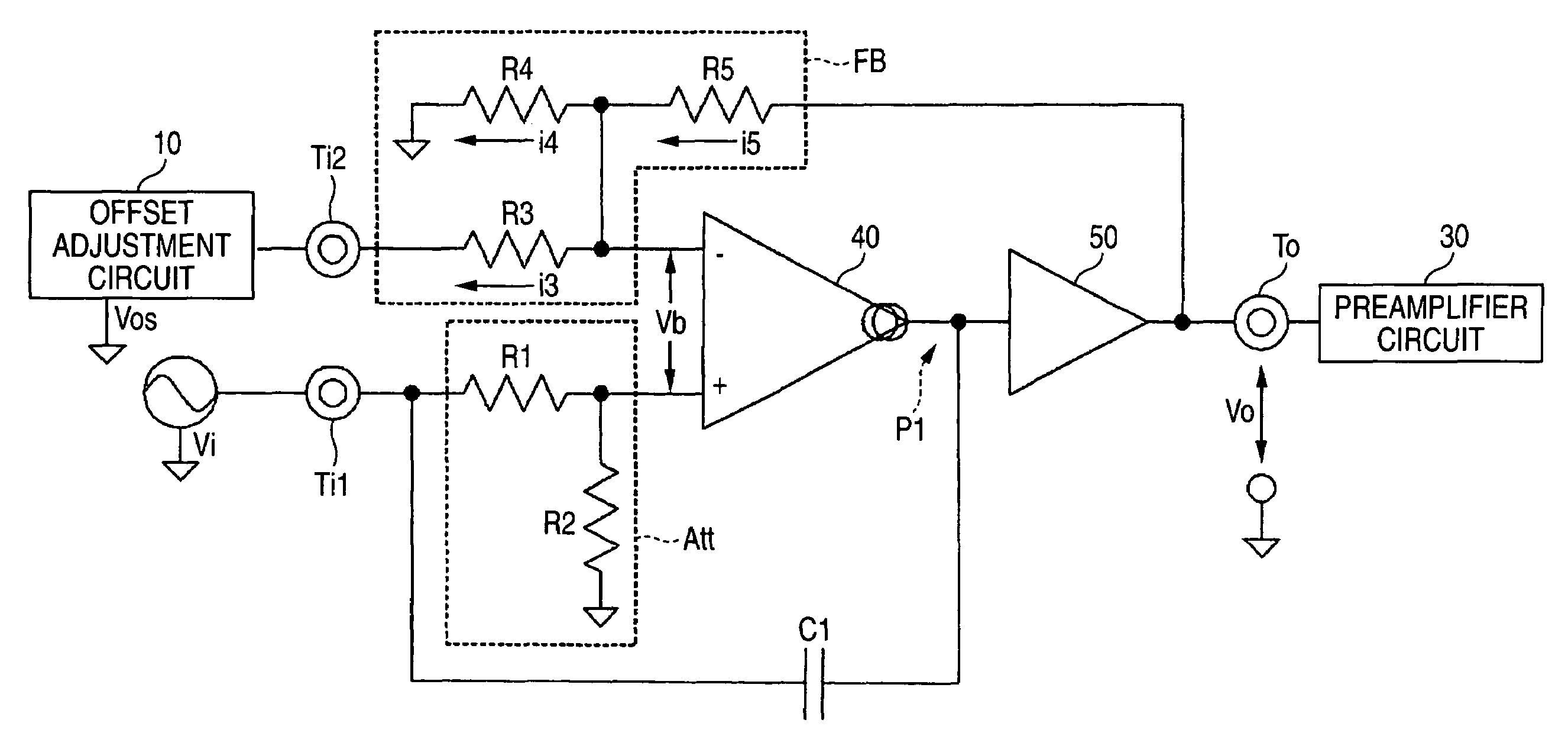
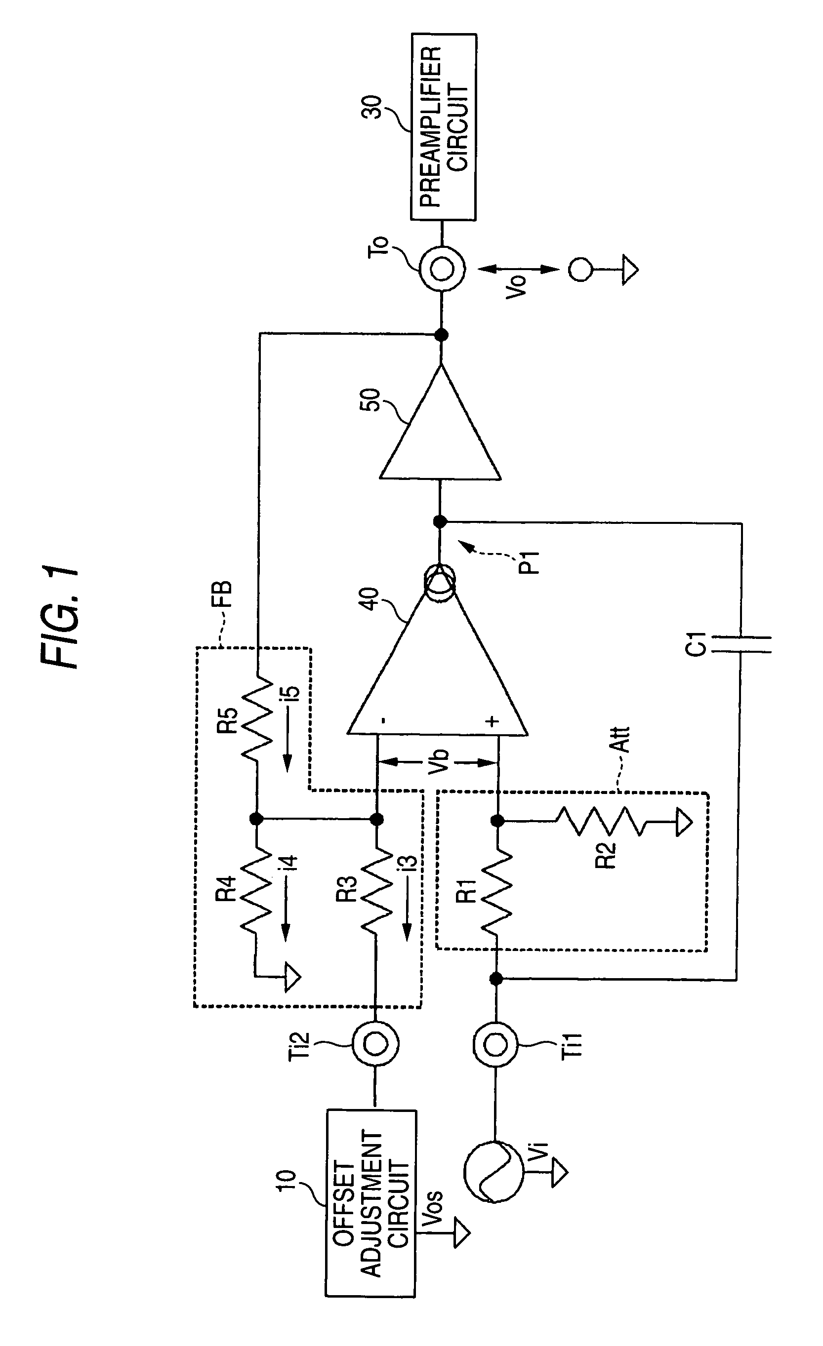
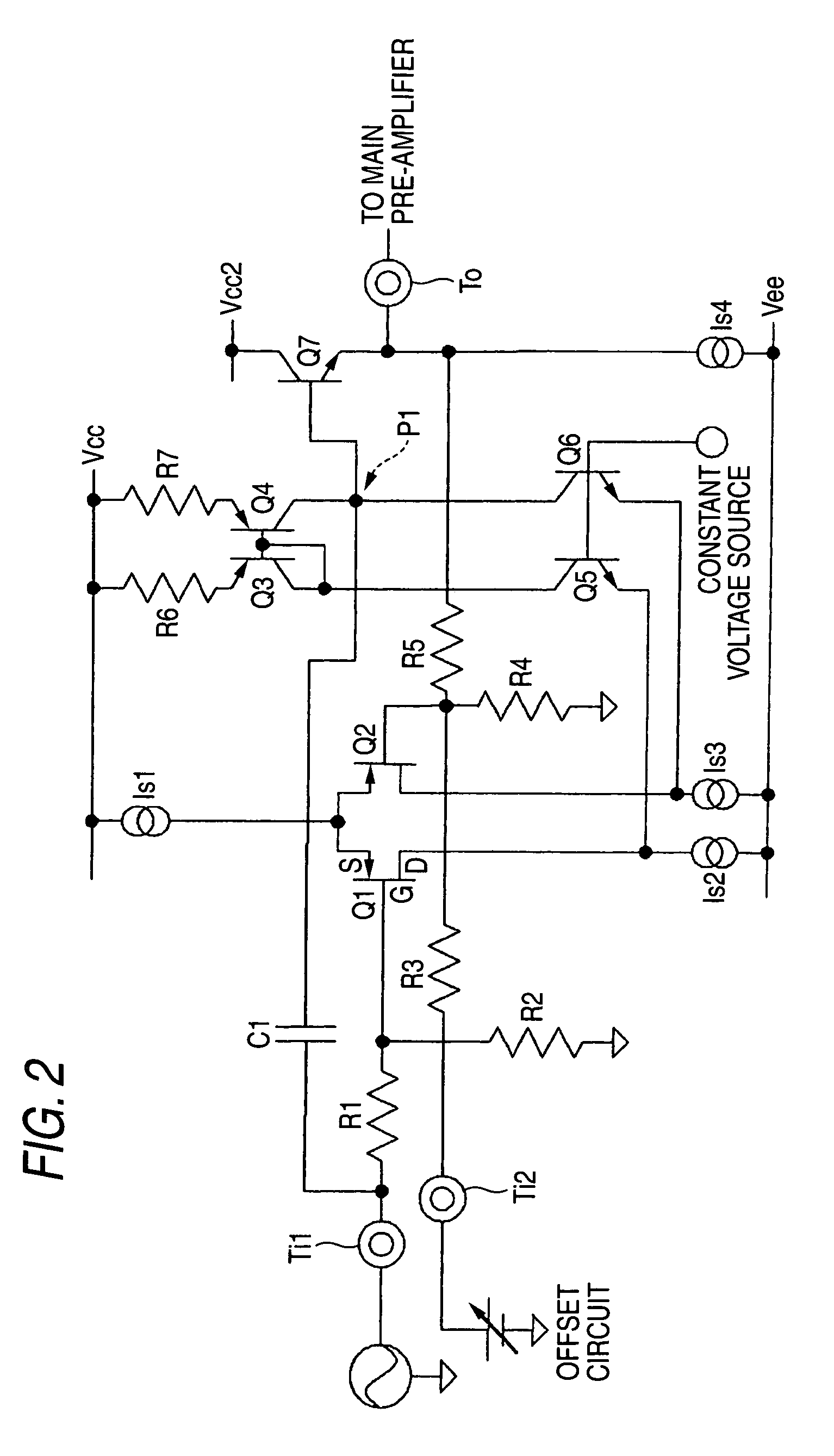
[0042]FIG. 1 is a block diagram showing an input circuit according to one embodiment of the invention. FIG. 2 is a circuit diagram of the input circuit as shown in FIG. 1. The same reference numbers will be used throughout the drawings to refer to the same or like parts. The description for the parts as already described in FIGS. 3 and 4 is omitted here. A differential amplification circuit 40 in place of the differential amplification circuit 20, a buffer 50, an attenuation circuit Att, a feedback circuit FB, and a capacitor C1 are provided. The differential amplification circuit 40 has a differential pair of p-channel MOS-FETs at the first stage, with two inputs and one output, and converts a differential signal into a single end signal to output the current. The buffer 50 has the input side connected to the output side of the differential amplification circuit 40, and ...


PUM


Abstract

An input circuit has a differential amplification circuit which converts a differential signal to a single end signal to output the single end signal, an attenuation circuit which attenuates a first input signal to output the attenuated signal to the differential amplification circuit, a capacitor in which one end thereof is connected to a first input terminal to which the first input signal is inputted, and another end thereof is connected to an output side of the differential amplification circuit, a buffer to which the single end signal outputted from the differential amplification circuit and a signal transmitted through the capacitor are inputted, and which outputs the output signal, and a feedback circuit which outputs a signal based on an output signal outputted from the buffer and the second input signal to the differential amplification circuit.

Description

CROSS-REFERENCE TO RELATED APPLICATIONS[0001]This application is based upon the prior Japanese Patent Applications No. 2003-424761, filed on Dec. 22, 2003, the entire contents of which are incorporated herein by reference.BACKGROUND OF THE INVENTION[0002]1. Field of the Invention[0003]The present invention relates to an input circuit to which a first input signal and a second input signal are inputted from two input terminals and which outputs an output signal acquired by performing differential amplification of the first input signal and the second input signal from an output terminal. The present invention particularly relates to an input circuit which has a wide band of frequency characteristic and a large voltage range for input, with a high input impedance.[0004]2. Description of the Related Art[0005]The input circuits for the electronic measurement apparatuses, including an oscilloscope, need a so-called buffer amplifier for buffering to be less affected by the measured system...

Claims


Application Information

Patent Timeline
17 Oct 2006
Publication
US7123080B2
IPC
H03F3/45; H03F1/34
CPC
H03F3/189; H03F3/45192
Inventors
FURUKAWA, ATSUSHI; SAITO, TAKUYA