Optical device and method of producing the same
a technology of optical devices and optical fiber arrays, applied in the field of optical devices, can solve the problems of insufficient mechanical strength of the member 208, inability to use optical devices, and difficulty in realizing an optical device of a relatively small size, and achieve the effects of reducing the attenuation of signal lights, and reducing the size of optical devices
- Summary
- Abstract
- Description
- Claims
- Application Information
AI Technical Summary
Benefits of technology
Problems solved by technology
Method used
Image
Examples
first embodiment
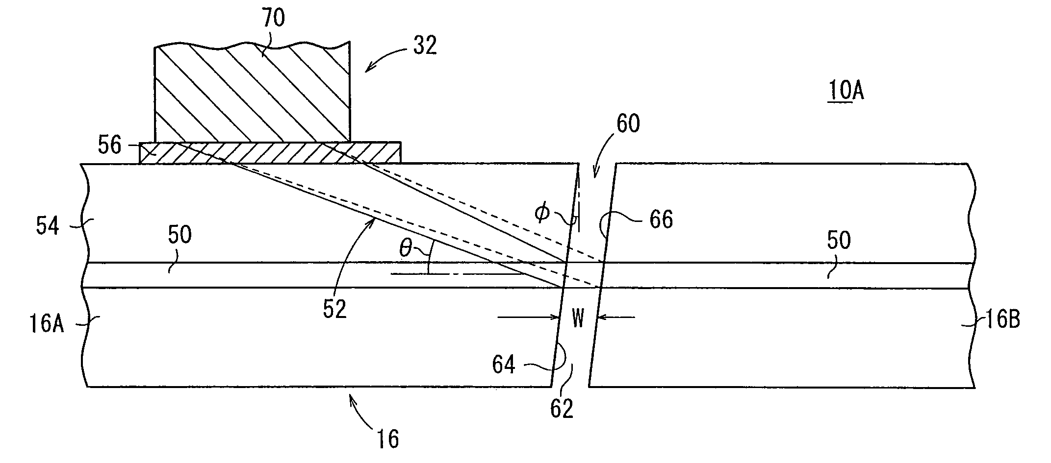
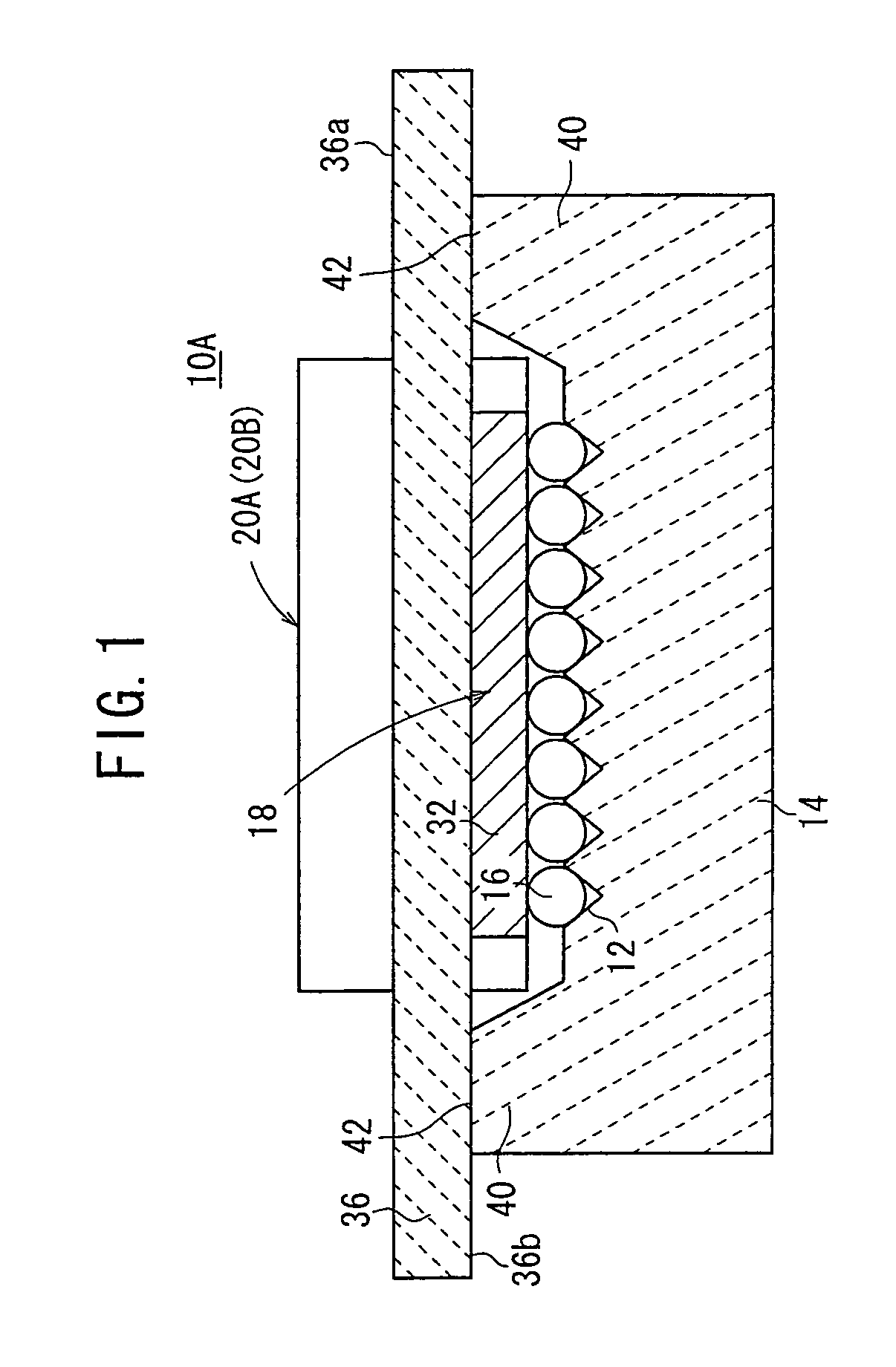
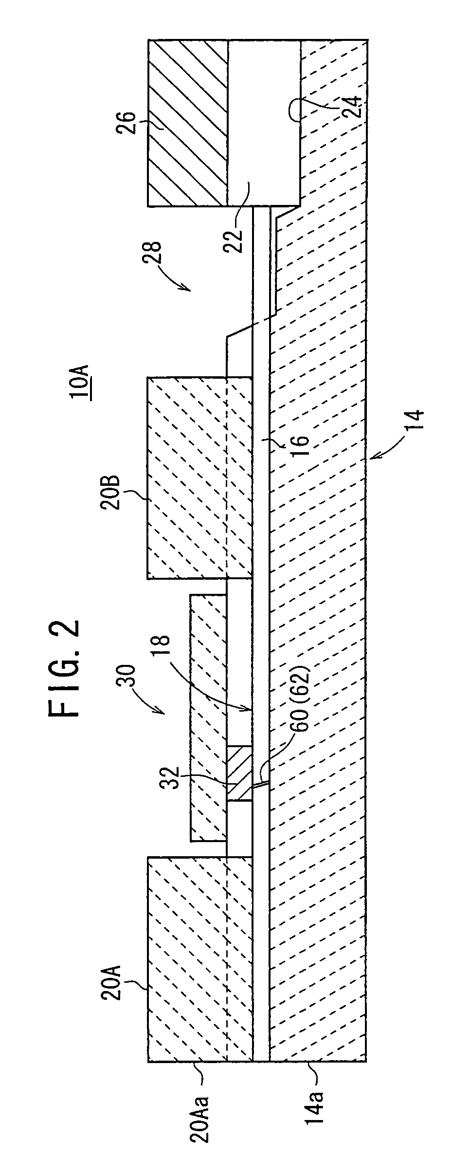
[0155]At first, as shown in FIGS. 1 and 2, an optical device 10A has a substrate 14 including a plurality of (eight, in the illustrated embodiment) V-grooves 12 which are formed in parallel on the upper surface of the substrate 14. A plurality of optical fibers 16 is fixed on the V-grooves 12. That is, an optical fiber array 18, which comprises the plurality of optical fibers 16 arranged on the V-grooves 12, is fixed on the substrate 14.
[0156]Two plates (first and second plates 20A, 20B) for holding the optical fiber array 18 are secured on the optical fiber array 18 so that the optical fiber array 18 is fixed onto the V-grooves 12 by the two plates 20A, 20B. The first plate 20A is fixed on the optical fiber array 18 so that an end surface 20Aa of the first plate 20A is substantially flush with an end surface 14a of the substrate 14. The second plate 20B is fixed on the optical fiber array 18 so that the second plate 20B is at a distance from the first plate 20A.
[0157]A surface 24 ...
second embodiment
[0176]Next, an optical device 10B will be explained with reference to FIG. 5.
[0177]The optical device 10B according to the second embodiment has approximately the same construction as the optical device 10A according to the first embodiment described above. However, the optical device 10B has a total reflection plane 80, which is formed in the clad 54 of the rear fiber 16A and which changes the optical path of the reflected light 52.
[0178]That is, a low refractive index layer (total reflection layer 82) for generating the total reflection of the reflected light 52 is provided in the rear fiber 16A separately from the reflective layer as described above. In the embodiment shown in FIG. 5, the total reflection layer (slit) 82 having an angle to generate the total reflection of the reflected light 52, is provided on the optical path of the reflected light 52 in the clad 54 of the rear fiber 16A. The total reflection layer 82 is an air layer. Therefore, the reflected light 52, which co...
third embodiment
[0185]Next, an optical device 10C will be explained with reference to FIG. 6.
[0186]The optical device 10C according to the third embodiment has approximately the same construction as the optical device 10A according to the first embodiment described above. However, the optical device 10C has a mirror member 90 mounted outside the rear fiber 16A. A mirror surface 90a of the mirror member 90 constitutes a reflection plane which changes the optical path of the reflected light 52 obtained through the layer 56.
[0187]The reflected light 52 is not transmitted through the interior of the mirror member 90. The reflected light 52 is totally reflected by the mirror surface 90a, and it arrives at the light-receiving surface of the photodetectors 70. In this embodiment, it is also necessary to provide the layer 56 in order to avoid the total reflection on the interface of the clad 54. The reflected light 52 is transmitted through the layer 56, and it is reflected by the mirror surface 90a. Ther...
PUM
 Abstract
Description
Claims
Application Information


