Processor architecture with independently addressable memory banks for storing instructions to be executed

a processing device and memory bank technology, applied in the direction of memory adressing/allocation/relocation, instruments, program control, etc., can solve the problems of memory bottleneck, comparatively expensive cache memory, and restricting the overall speed of the processing device, and achieve the effect of less overhead

Inactive Publication Date: 2006-10-17
SAMSUNG ELECTRONICS CO LTD
View PDF3 Cites 24 Cited by
  • Summary
  • Abstract
  • Description
  • Claims
  • Application Information

AI Technical Summary

Benefits of technology

[0011]It is, inter alia, an object of the invention to provide a process...

Problems solved by technology

Therefore, if no special steps are taken, the memory is a restrictive factor in respect of the overall speed of the processing device.
This problem is called the “memory bottleneck”.
The cache memory is comparatively expensive, because it must be sufficiently fast to read...

Method used


Image

  • Processor architecture with independently addressable memory banks for storing instructions to be executed
  • Processor architecture with independently addressable memory banks for storing instructions to be executed
  • Processor architecture with independently addressable memory banks for storing instructions to be executed

Examples


Embodiment Construction

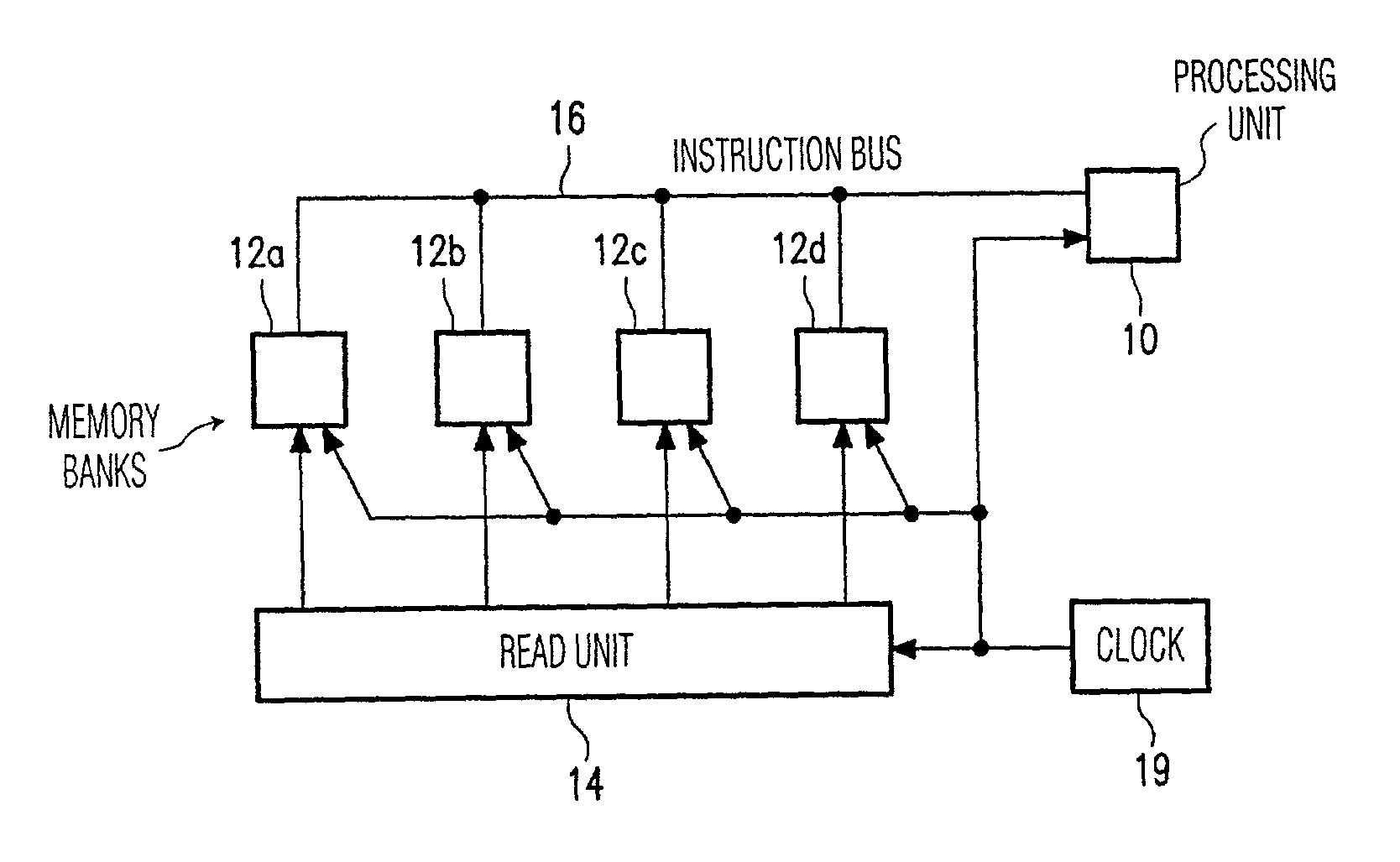
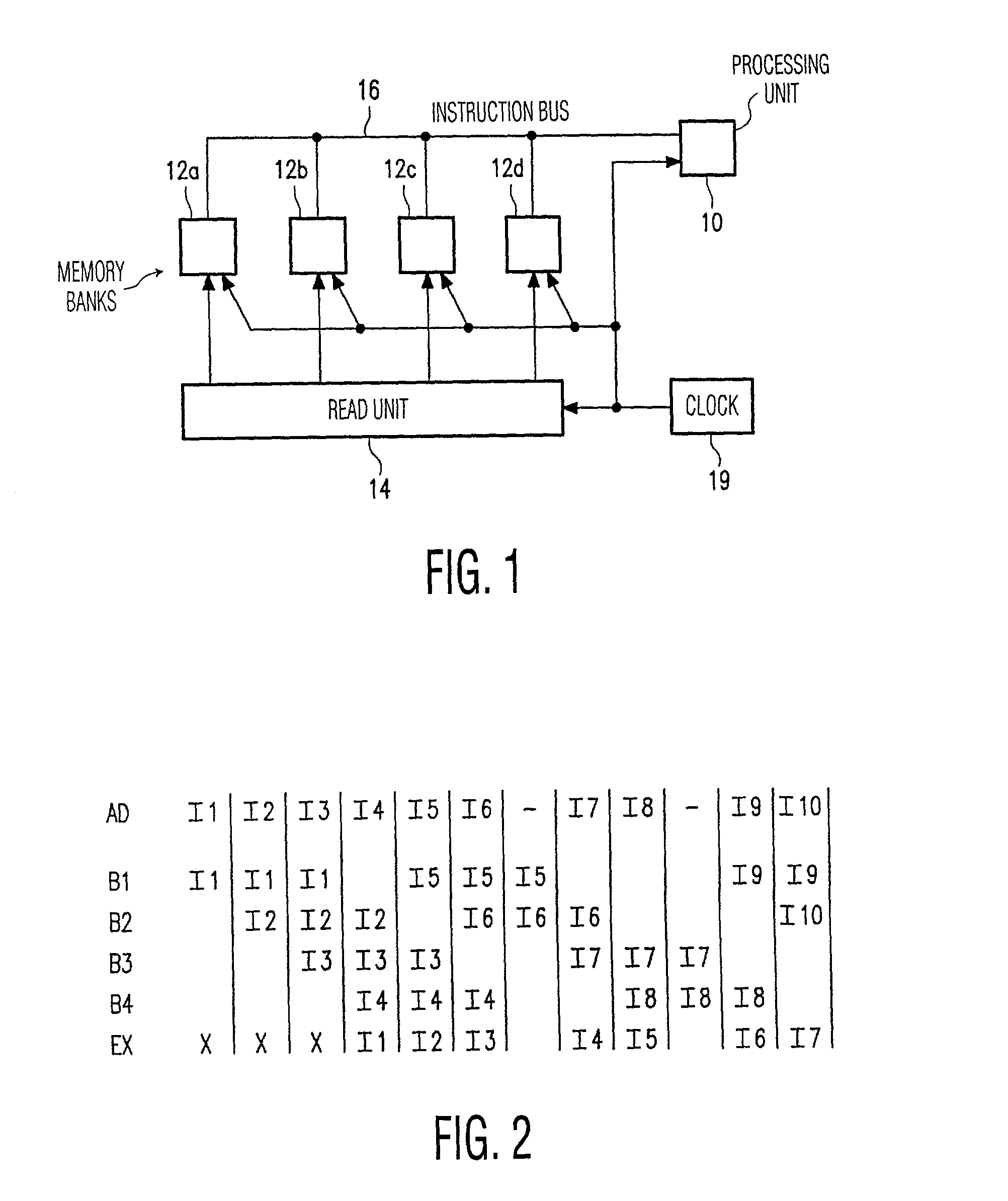
[0028]FIG. 1 shows an embodiment of a processing device according to the invention. The processing device includes a processing unit 10, a memory with a number of memory banks 12a–d, a read unit 14 and a clock 19. The read unit 14 has a number of address / selection outputs, each of which is coupled to a respective memory bank 12a–d via an associated address / selection connection 18a–d. The memory banks 12a–d are connected to an instruction input of the processing unit 10 via an instruction bus 16. The clock 19 is coupled to the read unit 14, the memory banks 12a–d and the processing unit 10.

[0029]FIG. 2 shows a timing diagram relating to the operation of the processing device shown in FIG. 1. The read unit 14 addresses successive memory locations in successive clock periods (also referred to as instruction cycles or read cycles). The trace bearing the label AD indicates per clock period which memory address (I1, I2, . . . ) has been selected Memory locations having successive memory a...


PUM


Abstract

Instructions for a processing unit are stored in a number of memory banks, successive instructions being stored in successive, different memory banks. Whenever execution of an instruction is started, the reading of one instruction which will be executed more than one instruction cycle later is also started. Consequently, a plurality of instructions are read in parallel from different memory banks. After the reading of an instruction, and before starting the execution of the instruction, the instruction passes through a pipeline in which the processing device detects whether the relevant instruction is a branch instruction. If this is so, the processing unit starts the reading in parallel of a number of instructions as from a branch target instruction. If it appears at a later stage that the branch is taken, said number of instructions is loaded into the pipeline in parallel.

Description

[0001]The present application is a continuation application claiming the benefit of U.S. patent application Ser. No. 08 / 963,937 filed Nov. 4, 1997, and issued Mar. 19, 2002, as U.S. Pat. No. 6,360,311.BACKGROUND OF THE INVENTION[0002]1. Field of the Invention[0003]The invention relates to a processing device, including[0004]a processing unit,[0005]a memory for storing instructions for the processing unit,[0006]a read unit for reading instructions from the memory in a logic sequence and for applying the instructions to the processing unit so as to be executed in the logic sequence.[0007]2. Related Art[0008]A processing device of this kind is known from International Patent Application No. WO 93 / 14457. During the execution of a program successive instructions are loaded from the memory into the processing unit so as to be executed. Contemporary processing units, however, are capable of executing the instructions faster, generally speaking, than the instructions can be read from the me...

Claims


Application Information

Patent Timeline
IPC IPC(8): G06F12/00G06F9/38G06F12/02G06F12/06
CPCG06F9/3804G06F12/0607G06F9/32
Inventor ZANDVELD, FREDERIKVLOT, MARNIX C.
Owner SAMSUNG ELECTRONICS CO LTD
Why Eureka
Try Eureka