Wire-bonding method and semiconductor package using the same

a technology of wire bonding and semiconductors, applied in semiconductor devices, semiconductor/solid-state device details, electrical devices, etc., can solve the problems of undesired increase in the thickness of the overall package, increase in the fabrication cost of the mold and the encapsulation process, and adversely increase the occurrence of short circuits, etc., to achieve eliminate drawbacks in the prior art, and reduce the cost of manufacturing

Active Publication Date: 2006-10-24
SILICONWARE PRECISION IND CO LTD
View PDF4 Cites 3 Cited by
  • Summary
  • Abstract
  • Description
  • Claims
  • Application Information

AI Technical Summary

Benefits of technology

[0008]A primary objective of the present invention is to provide a wire-bonding method and a semiconductor package using the same so as to improve the electrical quality of the semiconductor package.
[0010]Still another objective of the present invention is to provide a wire-boding method and a semiconductor package using the same, which can increase a pitch between adjacent bonding wires to prevent the adjacent wires from contact and short circuit with each other.
[0011]A further objective of the present invention is to provide a wire-bonding method and a semiconductor package using the same, which can reduce the affection of resin flow impact on bonding wires.
[0012]A further objective of the present invention is to provide a wire-bonding method that is easy to implement, and a semiconductor using the same.
[0017]Therefore, the wire-bonding method and the semiconductor package using the same proposed in the present invention, by provision of the second wires, have significant benefits as to preventing adjacent wires from contact and short circuit with each other due to wire sweep caused by the resin flow impact, as well as achieving profile miniaturization, simple fabrication processes and a high yield, such that the drawbacks in the prior art are eliminated.

Problems solved by technology

Therefore, it has become an important issue in the semiconductor industries to maintain relatively higher reliability of the bonding wires in wire-bonding and other fabrication processes.
This adversely increases the occurrence of short circuit caused by undesirable contact between the adjacent densely-arranged wires.
However, this arrangement makes the largest loop height S of the wire 75 much greater than the original loop height (S-H) and the thickness of a chip 77, such that the overall package thickness would be undesirably increased, which not complies with the requirement of miniaturization in package size and also leads to increase in the fabrication cost on the mold and the encapsulation process.
However, this method only alters the loop shape of the wire 85 but not the pitch between the wire 85 and an adjacent wire.
As a result, if the resin flow impact is great enough, the wire 85 would still be swept or shifted to come into contact with the adjacent wire thereby leading to short circuit and decreasing the production yield.
Further, U.S. Pat. No. 5,111,989 similarly discloses a wire-bonding method to control the shape of a wire loop, which however encounters the same drawbacks as U.S. Pat. No. 5,156,323 and is not able to solve the foregoing problems.

Method used


Image

  • Wire-bonding method and semiconductor package using the same
  • Wire-bonding method and semiconductor package using the same
  • Wire-bonding method and semiconductor package using the same

Examples


Embodiment Construction

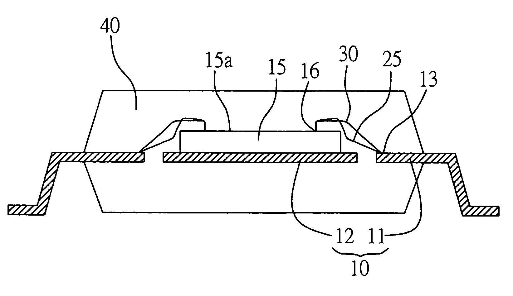
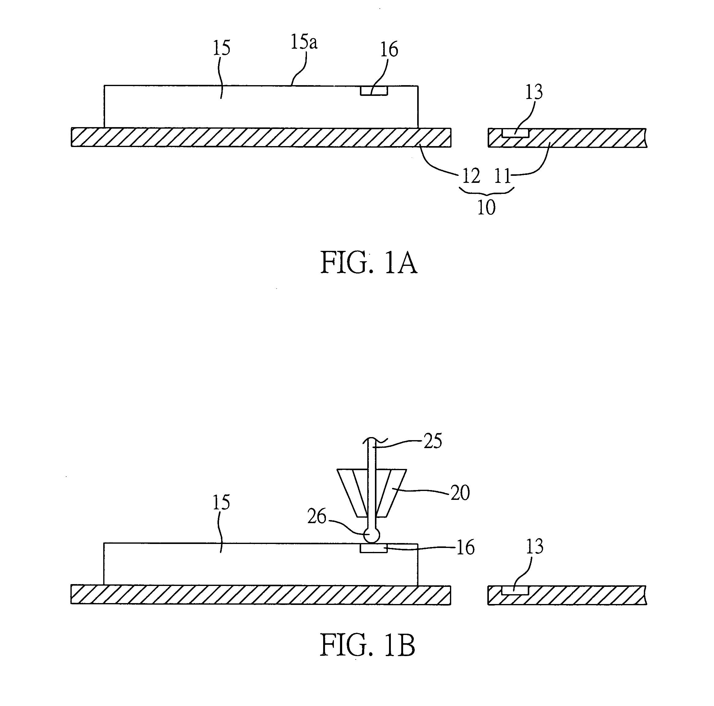
[0031]The following description exemplifies a semiconductor package using a lead frame as a carrier to illustrate a preferred embodiment of a wire-bonding method proposed in the present invention by which the fabricated wires are used to electrically connect a chip and a plurality of leads of the lead frame, with reference to in FIGS. 1A to 1F.

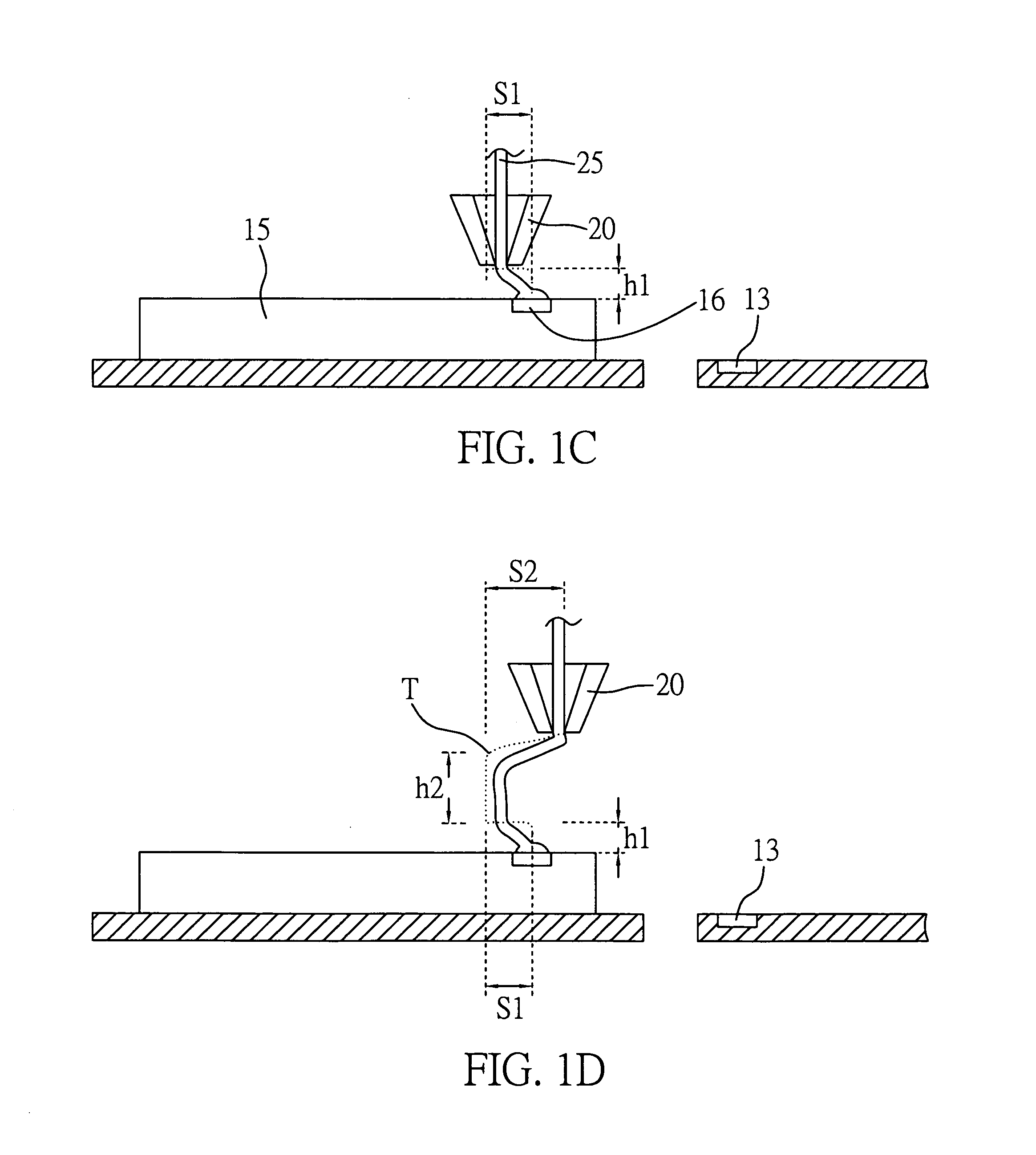
[0032]First, referring to FIG. 1A, the lead frame 10 having a die pad 12 mounted with the chip 15 thereon is prepared. The plurality of leads 11 of the lead frame 10 and an active surface 15a of the chip 15 are formed with a plurality of second bonding points 13 and first bonding points 16, respectively. Referring to FIG. 1B, a wire bonder is used to perform the wire-bonding method, by which a wire 25 such as gold wire is placed in a thermal tolerant capillary 20 of the wire bonder. A FAB (free air ball) 26 is formed on an end of the wire 25 by a spark discharge technique and is pressed onto one of the first bonding points 16 on the chip 15 ma...


PUM


Abstract

A wire-bonding method and a semiconductor package using the same are provided. The semiconductor package includes a carrier; a chip mounted on the carrier; a plurality of first wires and second wires alternatively arranged in a stagger manner, with a wire loop of each second wire being downwardly bent to form a deformed portion so as to provide a height different between the wire loops of each first wire and each second wire, wherein the first and second wires electrically connect the chip to the carrier; and an encapsulant for encapsulating the chip, the first wires, the second wires and a portion of the carrier. The height difference between the wire loops of each first wire and each second wire increases a pitch between adjacent first and second wires thereby preventing the wires from contact and short circuit with each other due to wire sweep during an encapsulation process.

Description

FIELD OF THE INVENTION[0001]The present invention relates to wire-bonding methods and semiconductor packages using the methods, and more particularly, to a wire-bonding method to form bonding wires having different heights of wire loops of adjacent wires, and a semiconductor package using this wire-bonding method.BACKGROUND OF THE INVENTION[0002]Conventionally for electrical connection established between a chip and an external component in a semiconductor package by using wire-bonding technology, the quality of electrical connection and the distribution density of bonding wires are key factors to determine the reliability and performances of the semiconductor package. Therefore, it has become an important issue in the semiconductor industries to maintain relatively higher reliability of the bonding wires in wire-bonding and other fabrication processes.[0003]A conventional semiconductor package fabricated using the wire-bonding technology is shown in FIG. 7. In the case of having a ...

Claims


Application Information

Patent Timeline
Patent Type & Authority Patents(United States)
IPC IPC(8): H01L23/48H01L23/495H01L23/52H01L21/56
CPCH01L21/565H01L23/4952H01L24/48H01L24/85H01L2924/01033H01L24/49H01L2924/15311H01L2924/014H01L2924/01082H01L2924/01079H01L2924/01006H01L2924/01005H01L24/45H01L24/78H01L2224/45144H01L2224/4809H01L2224/48091H01L2224/48095H01L2224/48227H01L2224/48247H01L2224/48465H01L2224/48599H01L2224/49171H01L2224/78301H01L2224/85181H01L2924/00014H01L2924/00012H01L2924/00H01L2224/85205H01L2924/181H01L2224/85399H01L2224/05599
Inventor HSU, CHIN-TENGLAIO, MING-CHUNCHEN, HOLMANLI, CHUN-YUANTANG, FU-DI
Owner SILICONWARE PRECISION IND CO LTD
Why Eureka
Try Eureka