Semiconductor device, method of manufacturing the same, and phase shift mask

a semiconductor and semiconductor technology, applied in semiconductor/solid-state device testing/measurement, originals for photomechanical treatment, instruments, etc., can solve the problems of peeling between layers or cracks, too small manufacturing, stress concentration, etc., to prevent the increase of chip area, prevent peeling, and secure a high moisture resistance

Inactive Publication Date: 2006-10-31
FUJITSU SEMICON LTD
View PDF15 Cites 38 Cited by
  • Summary
  • Abstract
  • Description
  • Claims
  • Application Information

AI Technical Summary

Benefits of technology

[0010]The present invention is made in view of the above disadvantage, and its object is to provide a semiconductor device which can prevent the increase in chip area and secure a high moisture resistance while preventing peeling in a peripheral edge portion, and a method of manufacturing the same, and a phase shift mask usable in manufacturing and the like of the semiconductor device.
[0013]According to the present invention, since the sub-wall part is selectively formed between the main wall part and the integrated circuit part, a wall part selectively has a double structure of the main wall part and the sub-wall part. Therefore, even when large stress is concentrated on a corner of the semiconductor substrate or the like by adopting the damascene method, the stress is dispersed to the sub-wall part as well, by disposing the sub-wall part at the position where the stress is easily concentrated. Thereby, an elastic structure is formed at the position in which stress relaxation is not caused due to peeling between layers, a crack and the like. Consequently, it is possible to keep an entry ratio of moisture accompanied by the occurrence of the crack low, and to ensure a high moisture resistance. Further, since a part of the wires and a part of the metal films are substantially formed as the same layer, the metal film can be formed simultaneously with the wire. Hence, it is possible to avoid the increase in the number of processes.

Problems solved by technology

For this reason, some of wires, which are formed by forming a film for metal wire material and directly etching the film, are too small to manufacture.
However, when the damascene method is employed, Cu is sometimes used because of its low electric resistance and high resistance to electromigration.
The thermal stress is concentrated on a corner of the chip to cause stress concentration, and peeling between layers or a crack may occur at the corner of the chip.
When the crack is caused, moisture as a disturbance easily enters into the chip.
Therefore, the conventional semiconductor device to which the damascene method is adopted has a disadvantage that it is difficult to secure a sufficient moisture resistance.

Method used


Image

  • Semiconductor device, method of manufacturing the same, and phase shift mask
  • Semiconductor device, method of manufacturing the same, and phase shift mask
  • Semiconductor device, method of manufacturing the same, and phase shift mask

Examples


first embodiment

[0049

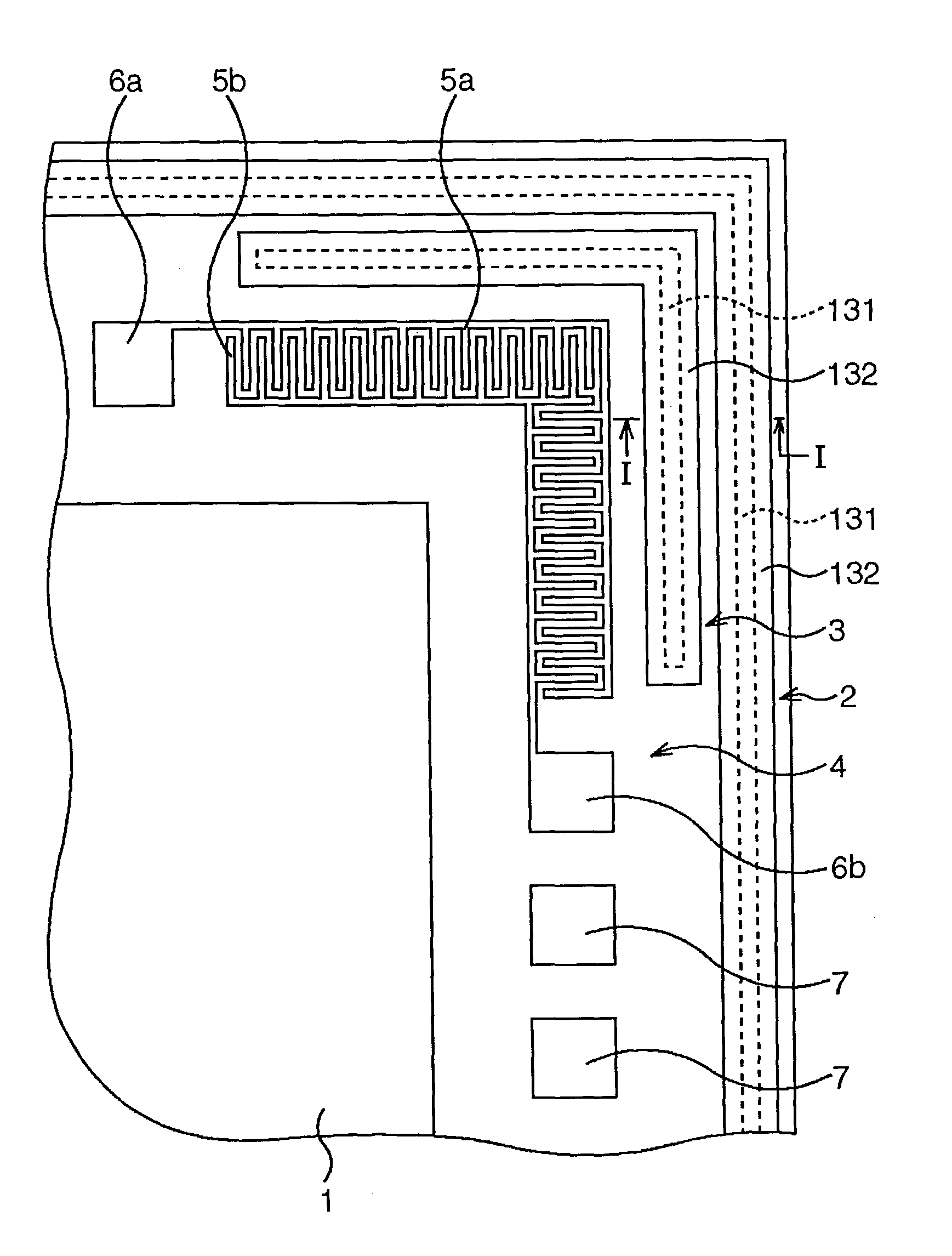
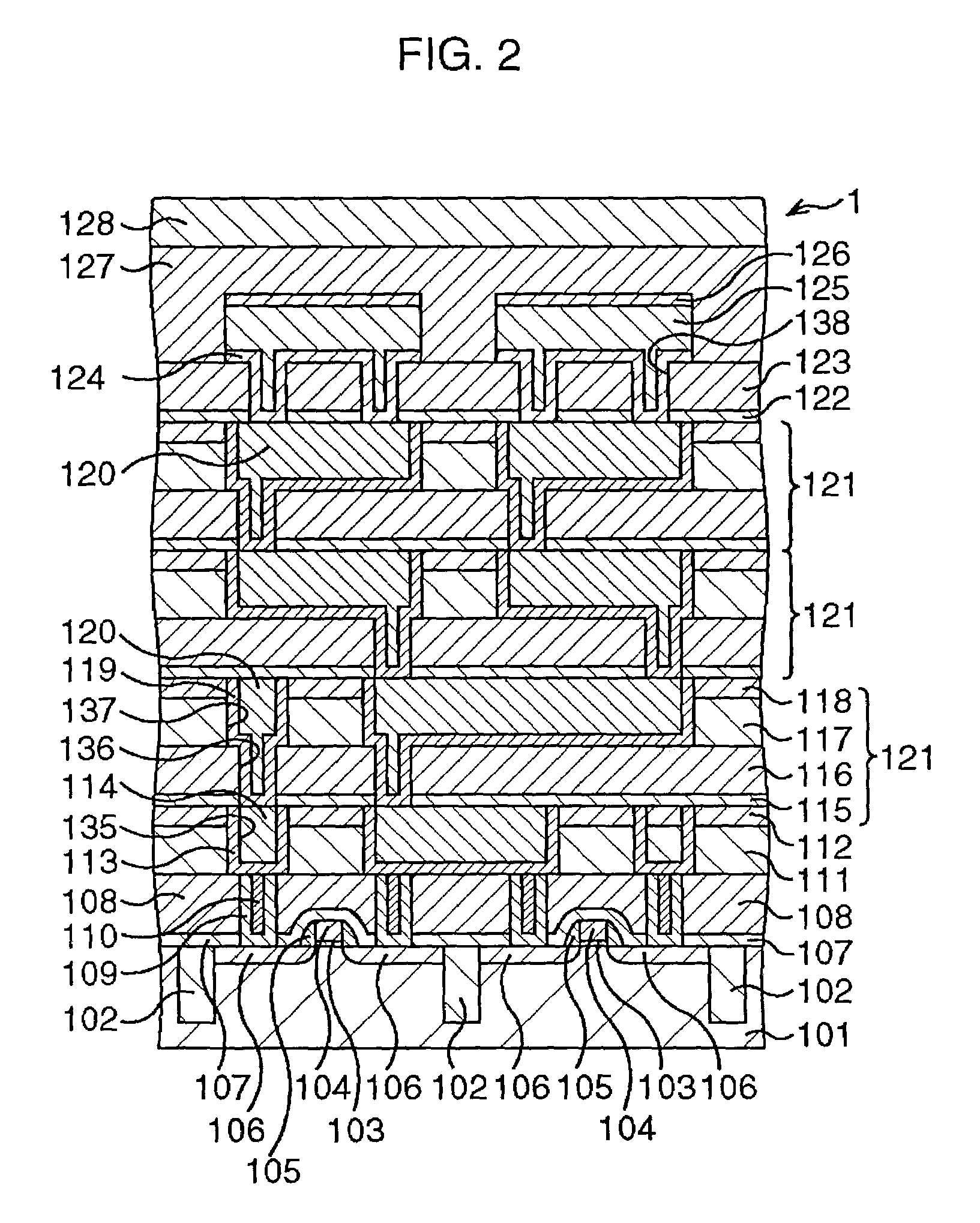
[0050]To begin with, a first embodiment of the present invention will be explained. FIG. 1 is a layout showing the structure of a semiconductor device according to the first embodiment of the present invention. FIG. 2 is a sectional view showing the structure of an integrated circuit part of the first embodiment, and FIG. 3 is a sectional view showing a section taken along the I—I line in FIG. 1. FIG. 4 is a layout showing the structure of a resistance value measuring part of the first embodiment, and FIG. 5 is a sectional view taken along the II—II line in FIG. 4.

[0051]According to the first embodiment, as shown in FIG. 1, a main wall part 2 which is, for example, in a rectangular shape is provided so as to surround an integrated circuit part 1 in which a semiconductor integrated circuit is formed. The semiconductor device according to this embodiment is diced along the main wall part 2 outside the main wall part 2, and is in a rectangular shape in plan view. A sub-wall part 3...

second embodiment

[0073

[0074]Next, a second embodiment of the present invention will be explained. FIG. 6 is a layout showing the structure of wall parts of a semiconductor device according to the second embodiment of the present invention.

[0075]According to the second embodiment, the structure of a sub-wall part is different from that of the first embodiment. In concrete, as shown in FIG. 6, the length of a narrow trench 131 and the length of a wide trench 132 in a sub-wall part 3a are the same with reference to a bending point, and, respective end parts are at the same positions in plan view. The structure of a section of each position of the sub-wall part 3a which crosses perpendicularly to a direction toward which the trenches extend is the same as that of the sub-wall part 3 in the first embodiment, except for the lengths of the trenches as described above. In this embodiment, the sub-wall part 3a is a first wall piece.

[0076]It is also possible to obtain the same effects as those of the first em...

third embodiment

[0077

[0078]Next, a third embodiment of the present invention will be explained. FIG. 7 is a layout showing the structure of wall parts of a semiconductor device according to the third embodiment of the present invention.

[0079]According to the third embodiment as well, the structure of a sub-wall part is different from that of the first embodiment. In concrete, as shown in FIG. 7, a sub-wall part 3b has a plan shape in which both end parts of the sub-wall part 3 of the first embodiment are bent perpendicularly toward the main wall part 2 side and are connected to the main wall part 2. In addition, a narrow trench 131 in the sub-wall part 3b is connected to a narrow trench 131 in the main wall part 2, and a wide trench 132 in the sub-wall part 3b is connected to a wide trench 132 in the main wall part 2. The structure of a section of each position of the sub-wall part 3b which crosses perpendicularly to a direction toward which the trenches extend is the same as that of the sub-wall p...


PUM

PropertyMeasurementUnit
diameteraaaaaaaaaa
diameteraaaaaaaaaa
diameteraaaaaaaaaa

Abstract

A main wall part is provided so as to surround an integrated circuit part. A sub-wall part which is in “L” shape is provided between each corner of the main wall part and the integrated circuit part. Therefore, even if the stress is concentrated due to heat treatment or the like, the stress is dispersed to the main wall part and the sub-wall part, and hence peeling between layers and a crack are unlikely to occur, as compared with the conventional art. Further, even if the crack and the like occur at the corner, moisture from the outside hardly reaches the integrated circuit part when the main wall part and the sub-wall part are coupled to each other. For this reason, it is possible to ensure an extremely high moisture resistance.

Description

CROSS-REFERENCE TO RELATED APPLICATIONS[0001]This application is based upon and claims priority of Japanese Patent Application Nos. 2002-072737, filed on Mar. 15, 2002 and 2002-286687, filed on Sep. 30, 2002, the contents being incorporated herein by reference.BACKGROUND OF THE INVENTION[0002]1. Field of the Invention[0003]The present invention relates to a semiconductor device in which moisture resistance in a multilayered wire structure is improved and a method of manufacturing the same, and a phase shift mask usable in manufacturing the semiconductor device.[0004]2. Description of the Related Art[0005]In recent years, a design rule of the multilayered wire structure has a tendency to be reduced in size as the LSI makes its transition. For this reason, some of wires, which are formed by forming a film for metal wire material and directly etching the film, are too small to manufacture. Hence, the following method is adopted as the method of forming the wire. That is, after forming ...

Claims


Application Information

Patent Timeline
Patent Type & Authority Patents(United States)
IPC IPC(8): H01L23/544G03F1/32G03F1/68H01L21/027H01L21/3205H01L21/66H01L21/768H01L21/822H01L23/00H01L23/52H01L23/522H01L23/58H01L27/04
CPCG03F1/26H01L21/76811H01L21/76813H01L23/562H01L23/564H01L23/585G03F1/32H01L2221/1036H01L2924/01078H01L2924/3025H01L2924/0002H01L2924/00
Inventor WATANABE, KENICHIKAWANO, MICHIARINAMBA, HIROSHISUKEGAWA, KAZUOHASEGAWA, TAKUMISAWADA, TOYOJI
Owner FUJITSU SEMICON LTD
Why Eureka
Try Eureka