
Cache memory architecture and associated microprocessor design

a memory architecture and cache technology, applied in the field of cache and memory architecture, can solve the problems of reducing the potential gain of increasing the cache size, and affecting the performance of the cach

Inactive Publication Date: 2006-10-31
MICROSEMI STORAGE SOLUTIONS
View PDF7 Cites 3 Cited by
  • Summary
  • Abstract
  • Description
  • Claims
  • Application Information

AI Technical Summary

Benefits of technology

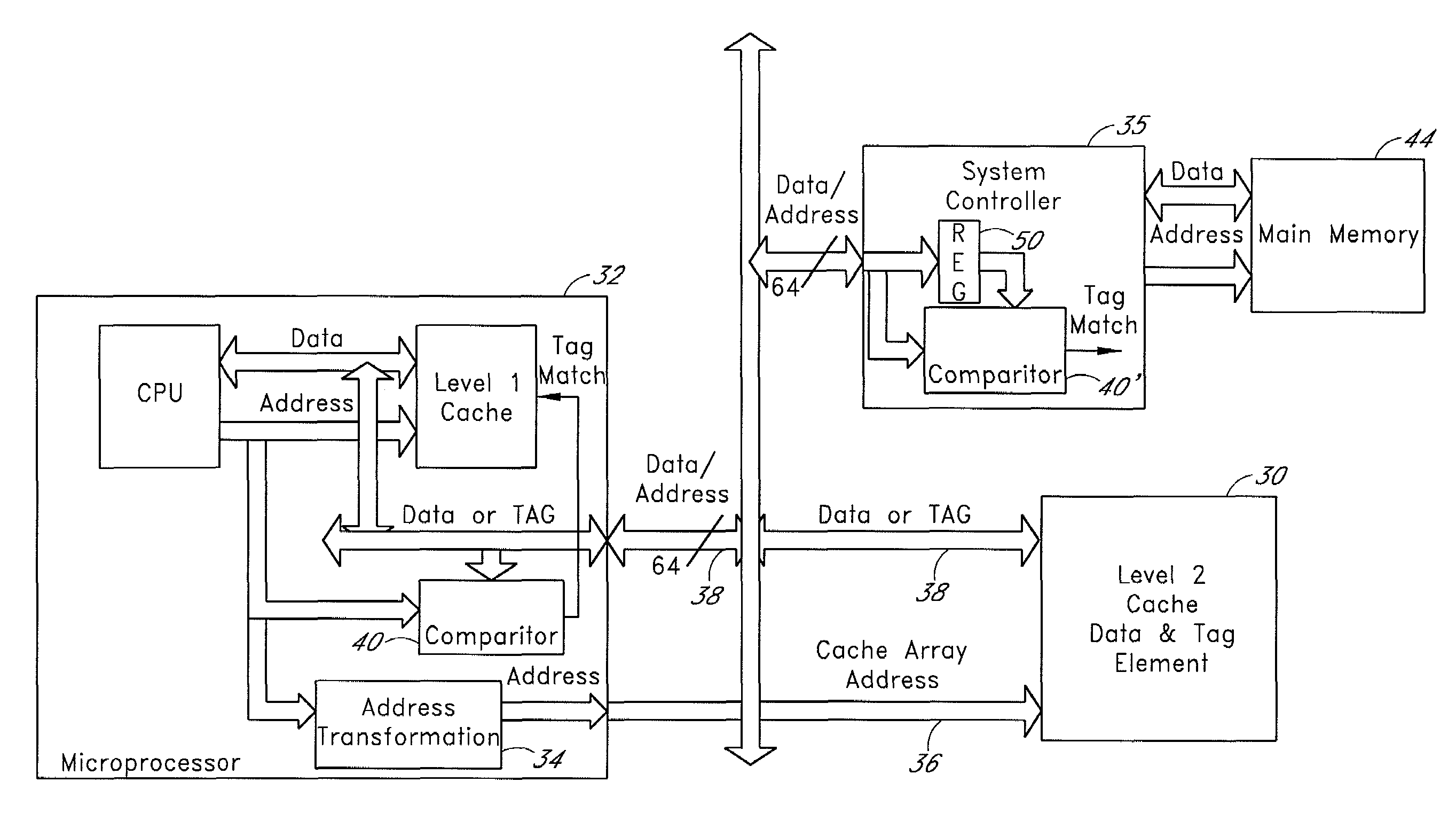
"The invention is a method and architecture for implementing a direct mapped cache using a single bank of SRAM for both tag and data elements. This eliminates the need for specialized tag functionality in the RAM arrays, allowing for the use of standard, general purpose SRAMs to store both cache tags and cache data. The invention reduces the system cost of a cache memory system built outside the microprocessor chip and provides a more efficient, lower cost implementation of high speed cache memory."

Problems solved by technology

Caches are, however, fundamentally different from main memories in some ways.
Cache design also focuses on the cost of implementation.
However, the larger RAM arrays needed for larger caches are typically slower than smaller arrays, negating some of the potential gain from increased cache sizes.
There are also definite physical barriers to desired cache implementations.
The size of a cache memory built on a microprocessor chip is limited by the costs and yield loss resulting from larger die sizes.
Off chip caches may more easily accommodate large cache sizes, but are limited by the restrictions on number of microprocessor chip pins that can be practically used to transfer addresses and data between the processor and the memory system.
Further, a multiplicity of chips may be required to implement the off-chip cache resulting in increased system cost.
Tag RAMs tend to be highly specialized to the particular application for which they are designed and thus tend to be significantly more expensive for the size of the arrays than are the more general purpose RAMs used for the data arrays.
The added cost is due largely to the addition of special tag comparison circuitry, as described above.
The use of tag RAMs thus adds a non-trivial additional cost to the implementation of these off chip caches.
With this approach, however, the microprocessor die size is increased by the area required for the tag RAM, resulting in significantly higher manufacturing costs.
In addition, the cost of the embedded tag RAM is incurred regardless of whether an external cache is actually implemented within the particular computer system.
As a result, these dual-function RAM devices are likely to be significantly more expensive than general purpose RAMs traditionally used for cache data arrays.
Another problem with the design of a cache memory system using separate data and tag arrays is that system designers typically cannot take advantage of advances in fabrication technology unless these advances have been incorporated into both types of memories.
For example, tag RAM chips that implement new electrical interface standards may not become commercially available until well after such interface standards have been incorporated into general purpose SRAM chips.

Method used


Image

  • Cache memory architecture and associated microprocessor design
  • Cache memory architecture and associated microprocessor design
  • Cache memory architecture and associated microprocessor design

Examples


Embodiment Construction

[0038]A particular embodiment will now be described in which an off-chip direct mapped cache is implemented with a single bank of SRAM memory chips. Control logic for the cache memory resides on the central processor chip and in the system memory controller. The processor provides the address used to access the cache and also supplies the address of the access to the system control chip.

[0039]The cache RAM address provided by the processor is based on the main memory address (real address) as used by the processor. Rather than simply using a range of the memory address bits as is typical to cache memory applications, an address transformation circuit changes the real address into either a tag or data address using a mapping function. The mapping function distinguishes between tag accesses and data accesses. Because addresses are mapped differently for tag and data accesses, a single memory element or array (e.g., a single bank of RAM chips) may be used for both tags and data without...


PUM


Abstract

A single memory element, which may consist of general purpose SRAM chips, is used to implement both tag and data cache memory functions, resulting in an efficient, low cost implementation of high speed external cache memory. In one embodiment, a bank of general purpose random access memory used by a microprocessor as an external cache memory stores both cache tags and cache data in separate memory locations. During a read operation, the microprocessor retrieves a cache tag from the bank of general purpose random access memory before retrieving corresponding cache data therefrom, and compares the cache tag to a memory address to assess whether requested data resides within the cache memory. The microprocessor preferably accesses the bank of general purpose random access memory using a memory mapping function which maps the memory address into a cache tag address and a cache data address.

Description

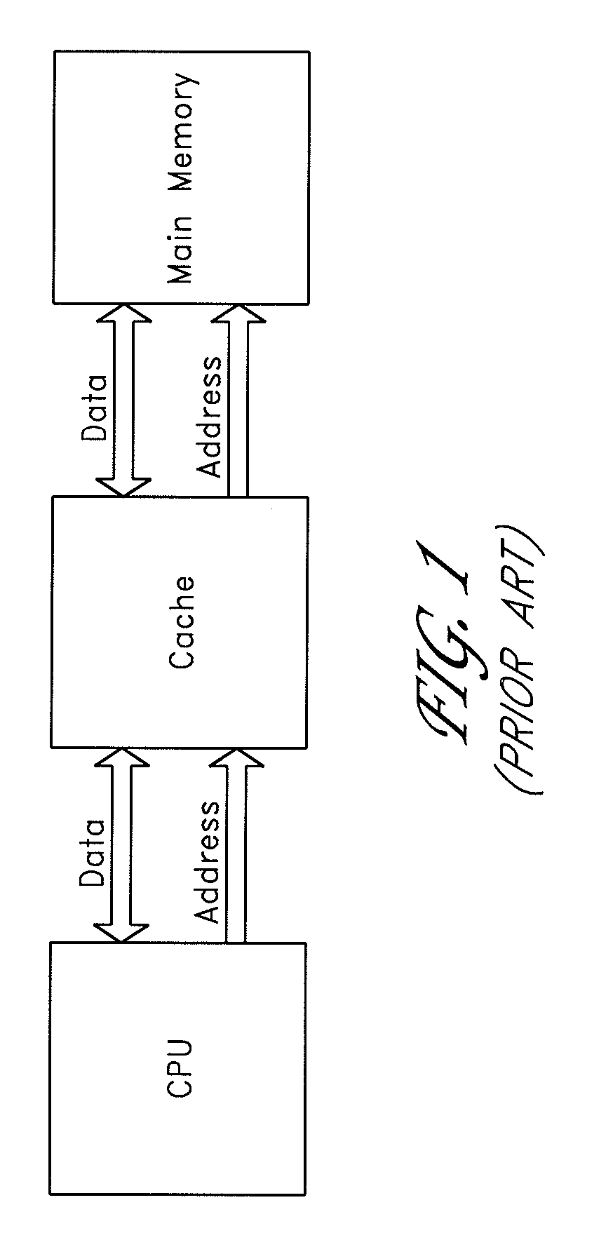
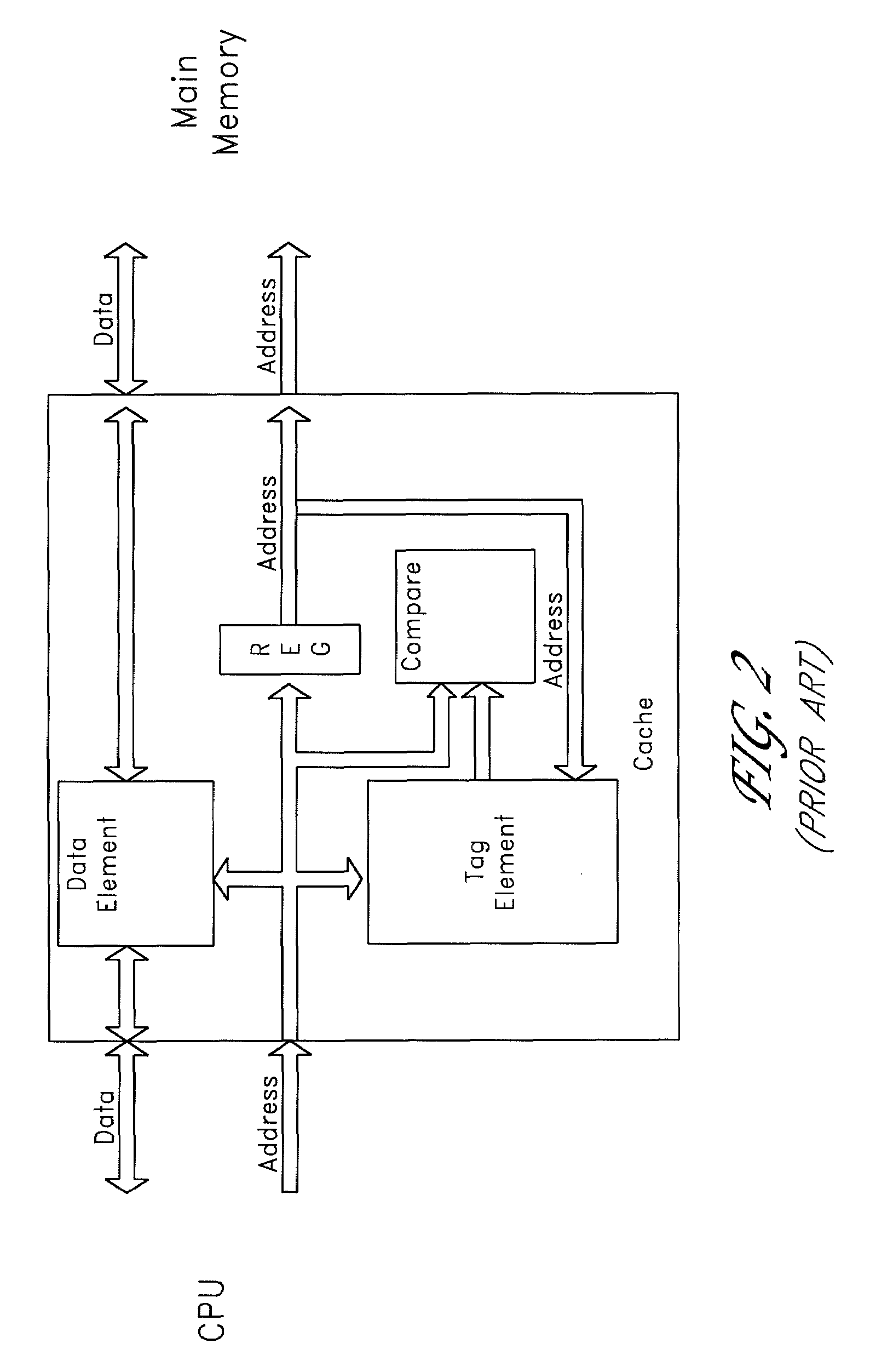
RELATED APPLICATIONS[0001]This application claims the benefit of U.S. Provisional Appl. No. 60 / 454,365, filed Mar. 11, 2003, the disclosure of which is hereby incorporated by reference.FIELD OF THE INVENTION[0002]The present invention relates to a cache, memory architecture in which cache data and tags are stored within a common external memory array, which may be implemented as a single bank of SRAM chips. The invention also relates to associated microprocessor and system controller circuitry for supporting the cache architecture.BACKGROUND OF THE INVENTION[0003]A cache memory provides a high speed interface between the Central Processing Unit (CPU) of a computer system and its main memory. As shown in FIG. 1, a smaller and faster cache memory provides the CPU high speed access to a larger, but slower main memory. The cache operates by maintaining a copy of those portions of the main memory's data that are likely to be used by the CPU. If the cache has the requested data, the CPU r...

Claims


Application Information

Patent Timeline
Patent Type & Authority Patents(United States)
IPC IPC(8): G06F12/10G06F12/08
CPCG06F12/0802
Inventor TAYLOR, MICHAEL DEMARKINSEL, JOHN R.RIORDAN, TOM
Owner MICROSEMI STORAGE SOLUTIONS
Learn More