Delay distribution calculation method, circuit evaluation method and false path extraction method

a delay distribution and calculation method technology, applied in the field of integrated circuit performance evaluation, can solve problems such as unnecessarily increasing area and costs, design including excessive margins, and inaccurate statistical analysis, and achieve the effect of calculating delay distribution more accurately

Inactive Publication Date: 2006-10-31
SOCIONEXT INC
View PDF19 Cites 8 Cited by
  • Summary
  • Abstract
  • Description
  • Claims
  • Application Information

AI Technical Summary

Benefits of technology

[0018]It is an object of the present invention to provide a method for calculating delay distribution of an integrated circuit, which is capable of calculating delay distribution more accurately according to an actual circuit.
[0019]It is another object of the present invention to provide an integrated circuit evaluation method having improved evaluation accuracy while avoiding effects of a false path. The present invention also proposes a method for extracting a false path from an integrated circuit to be designed.
[0021]According to the present invention, the delay distribution of the integrated circuit is calculated based on correlation information indicating a correlation of performance between the interconnects and elements that are included in the integrated circuit. This enables the delay distribution of the integrated circuit to be calculated with improved accuracy.
[0026]According to the present invention, evaluation can be conducted by using the equivalent circuit including no false path, allowing for rapid, accurate evaluation of performance of the integrated circuit.

Problems solved by technology

In delay calculation of a signal z in the circuit 100 as shown in FIG. 9, however, if the delays of signals x and y heavily depend on the delay of a signal b, there is a significant correlation between the delays of the signals x and y. If there is variation in interconnect delay, there is also a correlation between the signal transmission delays of fanout of the signal b. Accordingly, the statistical analysis that does not take correlation into account is likely to be inaccurate.
When delay distribution estimation has poor accuracy, it must be ensured that an integrated circuit will operate in a normal condition even under a plurality of worst conditions which are not likely to occur simultaneously in actual situations, resulting in design including excessive margins.
This unnecessarily increases the area and costs such as power consumption in the designed integrated circuit.
The conventional methods have additional problems.
This results in excessively increased calculation time, degraded accuracy in delay estimation, and the like.
However, if the specification does not allow simultaneous operation of the operating units, these series of operating units correspond to functional false paths.
It is practically impossible for human beings to find logical false paths in view of the large circuit scale.

Method used


Image

  • Delay distribution calculation method, circuit evaluation method and false path extraction method
  • Delay distribution calculation method, circuit evaluation method and false path extraction method
  • Delay distribution calculation method, circuit evaluation method and false path extraction method

Examples


first embodiment

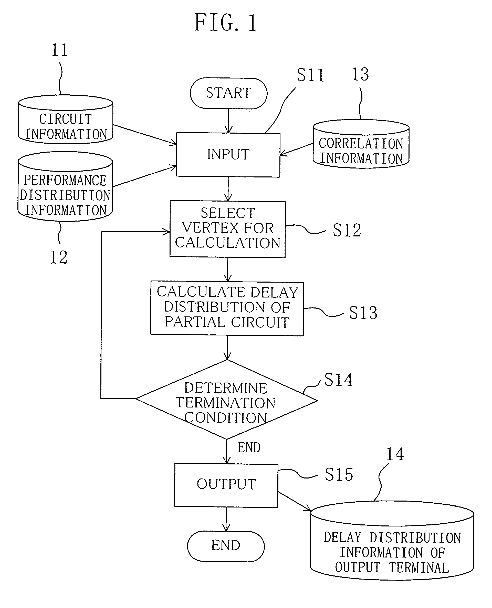
[0044]A method for calculating distribution of the maximum delay value for each terminal v of a circuit will be described in the first embodiment of the present invention. In the following description, d0(v) denotes the true maximum delay required to propagate a value “0” to a terminal v, and d1(v) denotes the true maximum delay required to propagate a value “1” to a terminal v.

[0045]First, a given circuit is represented by an acyclic graph G=(V, E) as shown in FIG. 10. For each edge e=(v, w), delay (weight of the edge e) t(e) required to transmit a signal value from a terminal v to a terminal w is regarded as a stochastic variable, and has a normal distribution N(μ, σ2). The mean μ and variance σ2 of the delay t(e) are respectively denoted by μ(e) and σ2(e). In other words, probability density function f(t(e)) of the delay t(e) is given by the following equation:

[0046]f⁡(t⁡(e))=12⁢π⁢σ⁡(e)⁢exp⁡[-(t⁡(e)-μ⁡(e))22⁢σ2⁡(e)].(1)

[0047]The delay t(e) of an edge e corresponding to an interco...

second embodiment

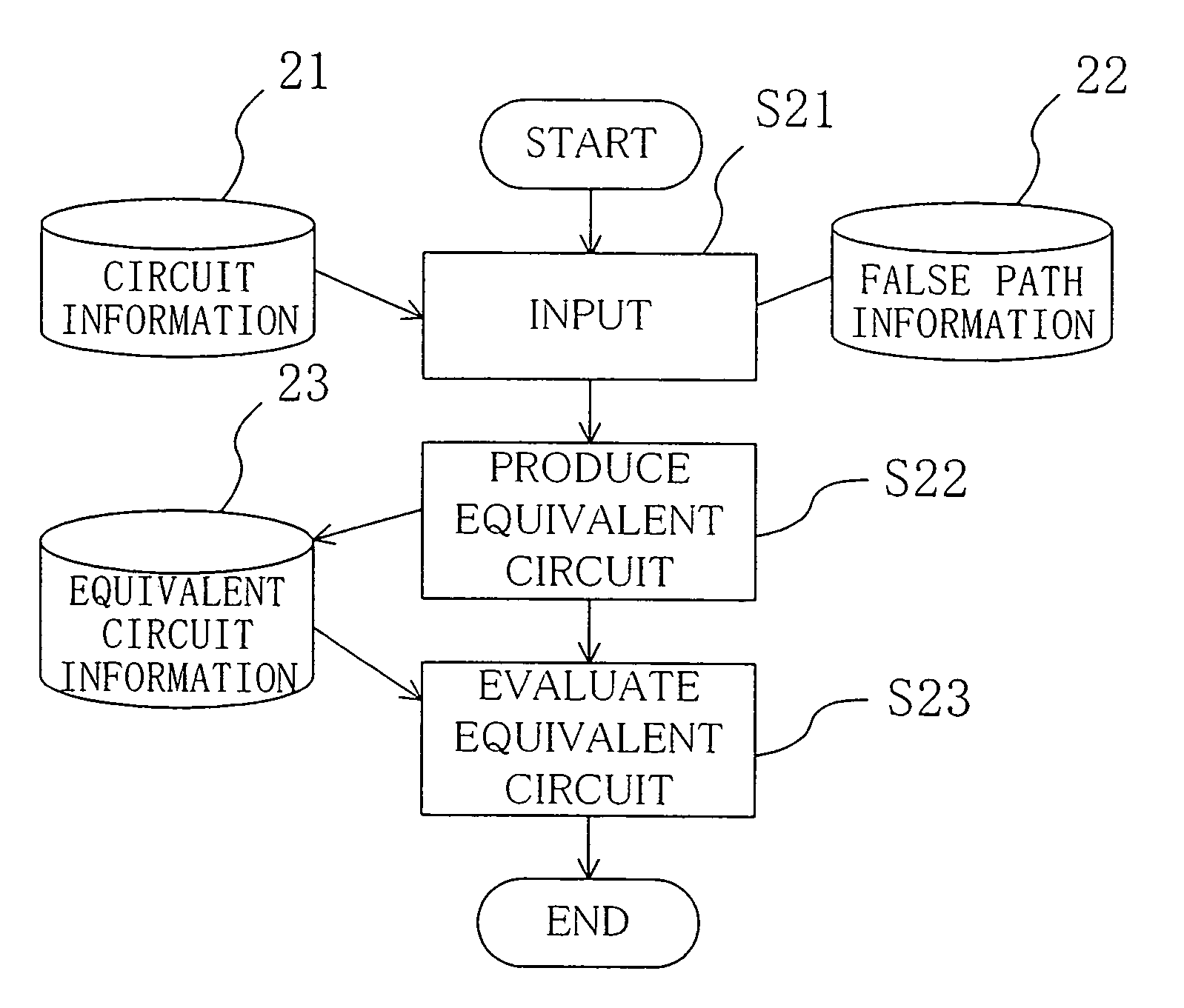
[0126]The second embodiment of the present invention relates to a method for evaluating a given circuit by removing false paths.

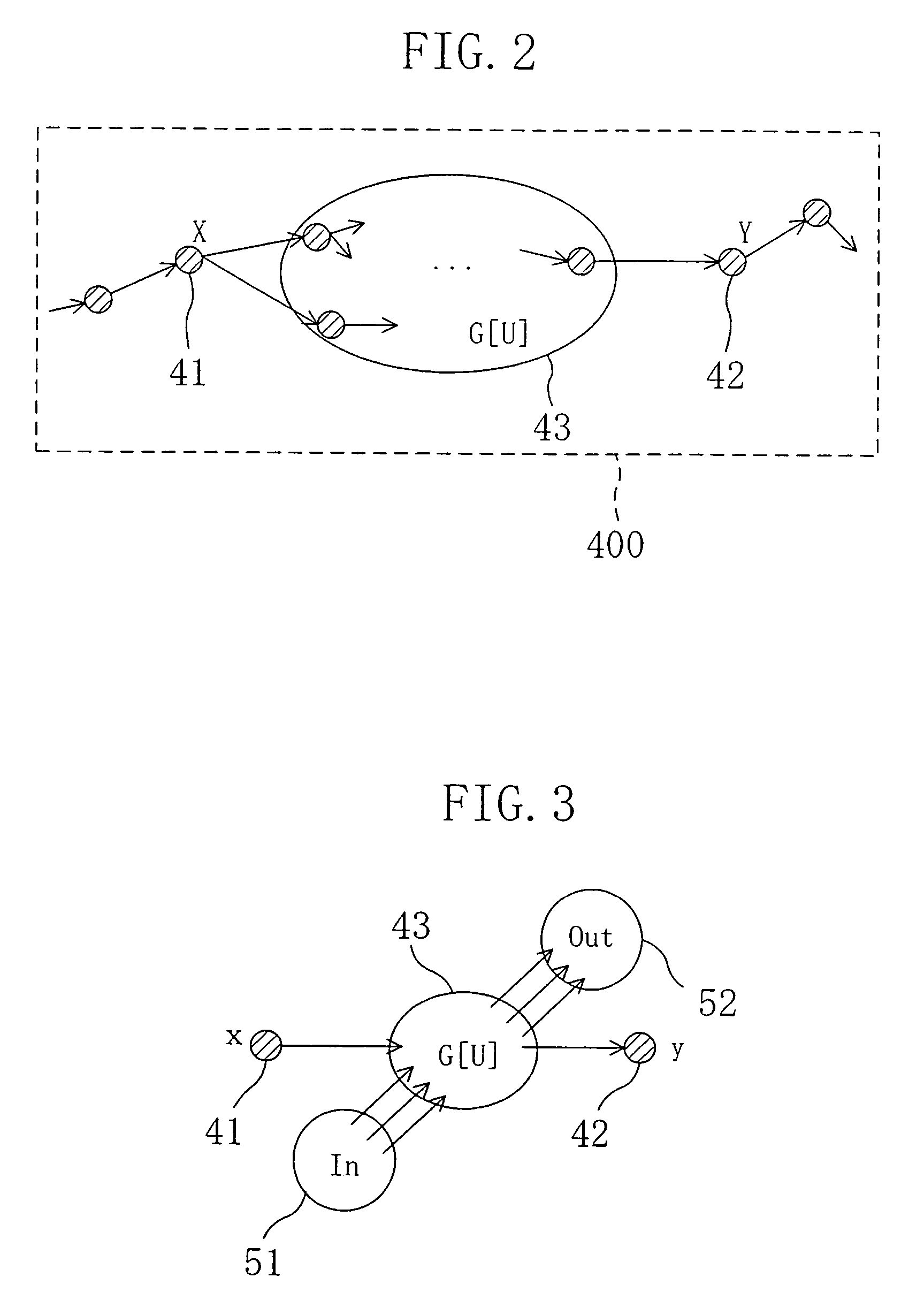
[0127]A “logical false path” can be characterized by using information on the connection structure of a circuit. In other words, a logical false path can be defined as a path passing through both two vertices x and y in an acyclic graph G=(V, E). A “functional false path” can be specified as a path including a causative path, and a causative path can be defined as a path from a vertex x of X to a vertex y of Y by using a pair of vertex sets (X, Y) (disclosed in H. C. Chen and D. H. Du, “Path sensitization in critical path problem,” IEEE Trans. Computer-Aided Design of ICs and Systems, vol. 12, no. 2, pp. 196–207, 1993).

[0128]More specifically, in FIG. 2, false paths can be designed as paths passing through both a vertex 41 of X and a vertex 42 of Y in a specified pair of vertex sets (X, Y). Therefore, removing these paths from the graph G 400 would enable i...


PUM


Abstract

Delay distribution in an integrated circuit is calculated while taking into account a correlation of performance between interconnects or elements in the integrated circuit, thereby improving estimation accuracy. Circuit information, performance distribution information of the interconnects or elements in the integrated circuit, and correlation information of performance between the interconnects or elements are input. A vertex is selected for calculation, and a correlation between delay distribution at the selected vertex and delay distribution in a partial circuit including the selected vertex is calculated based on the performance distribution information and the correlation information.

Description

[0001]This application is a divisional of application Ser. No. 09 / 988,602, filed Nov. 20, 2001, now U.S. Pat. No. 6,684,375.BACKGROUND OF THE INVENTION[0002]The present invention generally relates to technology of evaluating performance of an integrated circuit such as CMOS (Complementary Metal-Oxide Semiconductor) and LSI (Large Scale Integration) in its design. More particularly, the present invention relates to technology of calculation of delay distribution, and removal and extraction of false paths.[0003]In the VLSI (Very Large Scale Integration) design in deep sub-micron era, it is necessary to take variation in manufacturing process into account in advance so that circuits with required performance are produced with high yield. Like the technology such as OPC (Optical Proximity Correction), variation control by mask shape correction has become possible, and is increasingly required in practical applications. Therefore, the future VLSI physical design requires technology of de...

Claims


Application Information

Patent Timeline
Patent Type & Authority Patents(United States)
IPC IPC(8): G06F17/50G05B19/042
CPCG05B19/0421G06F17/50G06F17/5031G06F2217/10G06F2217/84G06F2111/08G06F30/3312G06F30/00G06F2119/12G06F30/3315
Inventor TSUKIYAMA, SHUJITANAKA, MASAKAZUFUKUI, MASAHIRO
Owner SOCIONEXT INC
Why Eureka
Try Eureka