

Method for treating surface of organic insulating film using helium plasma and method of fabricating thin film transistor substrate using the same
a technology of organic insulating film and surface treatment, which is applied in the direction of semiconductor devices, instruments, optics, etc., can solve the problems of insufficient adhesive strength of organic insulating film to transparent electrode material, critical defects, and insufficient adhesive strength of organic insulating film 26. , to achieve the effect of improving the adhesive strength of organic insulating film and improving yield
- Summary
- Abstract
- Description
- Claims
- Application Information
AI Technical Summary
Benefits of technology
Problems solved by technology
Method used
Image

Examples
Embodiment Construction
[0037]Reference will now be made in detail to the preferred embodiments of the present invention, examples of which are illustrated in the accompanying drawings. Whenever possible, the same reference numbers will be used throughout the drawings to refer the same or like parts.
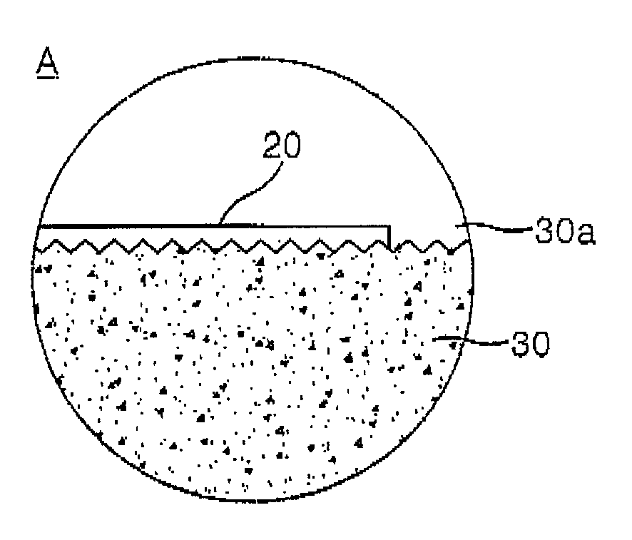
[0038]FIGS. 3A to 3C are sectional views sequentially illustrating a fabricating method of a thin film transistor substrate including the surface treatment method of an organic insulating film according to the preferred embodiment of the present invention.
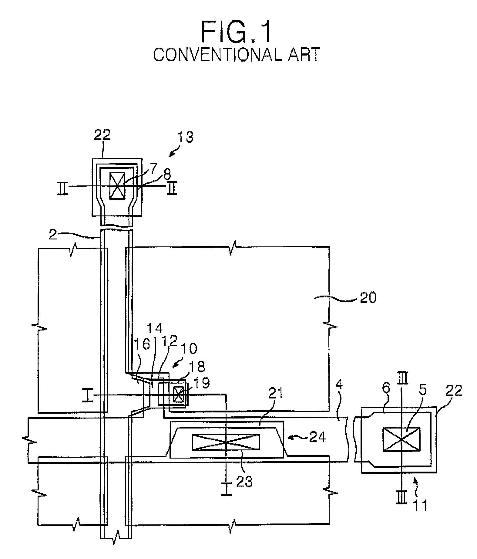
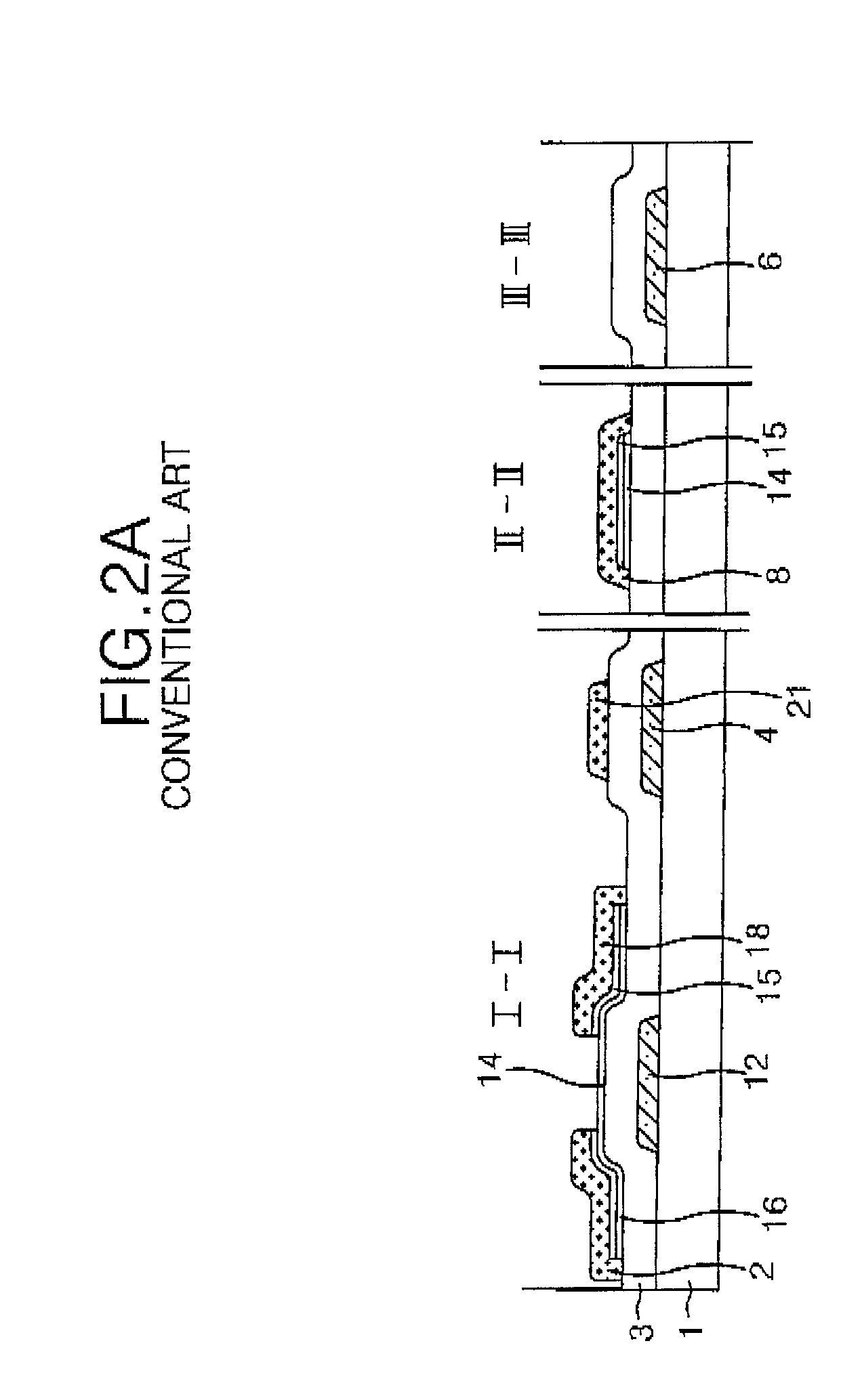
[0039]FIG. 3A illustrates a first step of the fabricating method of the thin film transistor substrate. As shown, there are formed gate patterns, source / drain patterns and a thin film transistor TFT 10 on a lower substrate 1. First, a gate metal layer is entirely deposited on the lower substrate 1 by a deposition method such as a sputtering technique or the like. Chromium (Cr), molybdenum (Mo), metal of aluminum system or the like may be used as the gate metal...
PUM
| Property | Measurement | Unit |
|---|---|---|
| adhesion | aaaaa | aaaaa |
| dielectric constant | aaaaa | aaaaa |
| atomic size | aaaaa | aaaaa |
Abstract
Description
Claims
Application Information