Apparatus and measurement procedure for the fast, quantitative, non-contact topographic investigation of semiconductor wafers and other mirror like surfaces

a technology of semiconductor wafers and measurement procedures, applied in the field of apparatus and process for fast, quantitative, non-contact topographic investigation of semiconductor wafers, can solve the problems of reducing the yield of manufactured circuits, affecting the quality of semiconductor wafers,

a technology of semiconductor wafers and measurement procedures, applied in the field of apparatus and process for fast, quantitative, non-contact topographic investigation of semiconductor wafers, can solve the problems of reducing the yield of manufactured circuits, affecting the quality of semiconductor wafers,

US7133140B2Inactive Publication Date: 2006-11-07HUNGARIAN ACAD OF SCI RES INST FOR TECHN PHYSICS & MATERIALS SCI +1

Image

  • Apparatus and measurement procedure for the fast, quantitative, non-contact topographic investigation of semiconductor wafers and other mirror like surfaces
  • Apparatus and measurement procedure for the fast, quantitative, non-contact topographic investigation of semiconductor wafers and other mirror like surfaces
  • Apparatus and measurement procedure for the fast, quantitative, non-contact topographic investigation of semiconductor wafers and other mirror like surfaces

Examples


Embodiment Construction

[0042]The particulars shown herein are by way of example and for purposes of illustrative discussion of the embodiments of the present invention only and are presented in the cause of providing what is believed to be the most useful and readily understood description of the principles and conceptual aspects of the present invention. In this regard, no attempt is made to show structural details of the present invention in more detail than is necessary for the fundamental understanding of the present invention, the description taken with the drawings making apparent to those skilled in the art how the several forms of the present invention may be embodied in practice.

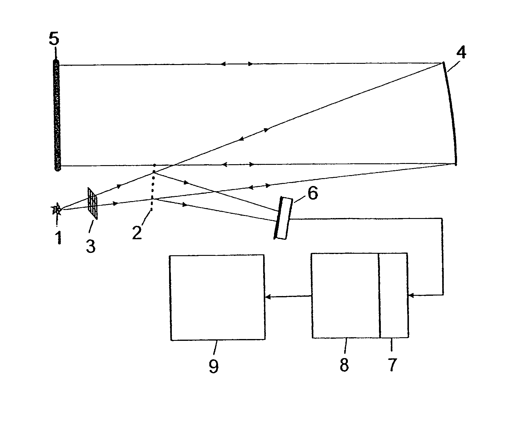
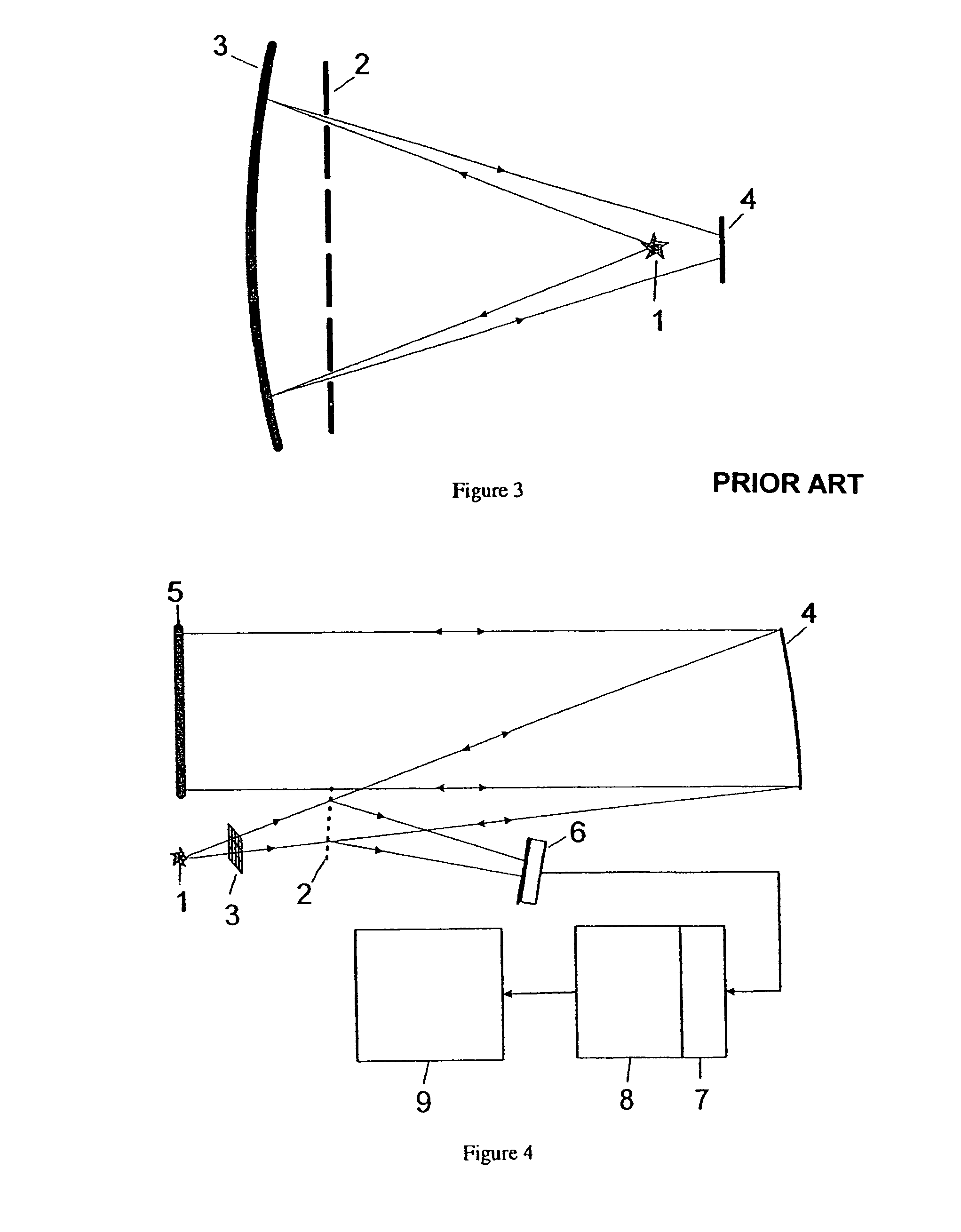
[0043]The present invention provides a measurement set-up for the non-contact, fast quantitative topographic investigation of semiconductor wafers and other mirror-like surfaces, as illustrated in FIG. 4. The set-up includes an essentially point light source 1, a concave mirror 4 that makes the beam of the light source pa...


PUM

PropertyMeasurementUnit
optical pathaaaaaaaaaa
semi-transparentaaaaaaaaaa
heightaaaaaaaaaa

Abstract

Apparatus and process for fast, quantitative, non-contact topographic investigation of samples. Apparatus includes a light source, and a collimating concave mirror structured and arranged to produce a parallel beam and to direct the parallel beam to a sample to be investigated. A structured mask is located between the light source and the concave mirror, and an image sensor structured and arranged to receive a beam reflected from the sample and the concave mirror. Relative positions of the mask and the sensor to other elements of the apparatus are chosen to provide an essentially sharp image of the mask on the sensor. The instant abstract is neither intended to define the invention disclosed in this specification nor intended to limit the scope of the invention in any way.

Description

CROSS-REFERENCE TO RELATED APPLICATIONS[0001]The present application is a continuation of International Patent Application No. PCT / EP02 / 11011 filed Oct. 1, 2002, the disclosure of which is expressly incorporated by reference herein in its entirety. The instant application further claims priority Hungarian Patent Application No. 0104057 filed Oct. 2, 2001.BACKGROUND OF THE INVENTION[0002]1. Field of the Invention[0003]The present invention is directed to an apparatus and process for fast, quantitative, non-contact topographic investigation of semiconductor wafers.[0004]2. Discussion of Background Information[0005]The microelectronics industry requires perfectly flat, mirror like surfaces having defect-free single-crystal wafers as a base for the production of integrated circuits and components. Any deviation from the ideal plane makes the manufacturing process difficult or even impossible or decreases the yield of the manufactured circuits. Such defects may often originate during the...

Claims


Application Information

Patent Timeline
07 Nov 2006
Publication
US7133140B2
IPC
G01B11/24
CPC
G01B11/303; G01N21/9501
Inventors
LUKÁCS, ISTVÁN ENDRE; MAKAI, JÁNOS