Integrated power devices and signal isolation structure

a power device and isolation structure technology, applied in semiconductor devices, semiconductor/solid-state device details, electrical devices, etc., can solve the problems of high-dose implants that cannot be integrated at high levels, thermal drives of high-dose implants are not feasible, and the surrounding implant region is distorted by thermal drives. high-dose implants can achieve high-dose implants, and achieve high-dose implants. the effect of high integration or prohibitively complex

Active Publication Date: 2006-11-14
QORVO US INC
View PDF16 Cites 103 Cited by
  • Summary
  • Abstract
  • Description
  • Claims
  • Application Information

AI Technical Summary

Problems solved by technology

However, for high levels of integration, the thermal drives of the high dose implants begin to distort nearby implant regions.
Thus, the thermal drives of high dose implants have not been feasible with high levels of integration or are prohibitively complex.
Further, adequate isolation is difficult to achieve.

Method used


Image

  • Integrated power devices and signal isolation structure
  • Integrated power devices and signal isolation structure
  • Integrated power devices and signal isolation structure

Examples


Embodiment Construction

[0010]The embodiments set forth below represent the necessary information to enable those skilled in the art to practice the invention and illustrate the best mode of practicing the invention. Upon reading the following description in light of the accompanying drawing figures, those skilled in the art will understand the concepts of the invention and will recognize applications of these concepts not particularly addressed herein. It should be understood that these concepts and applications fall within the scope of the disclosure and the accompanying claims.

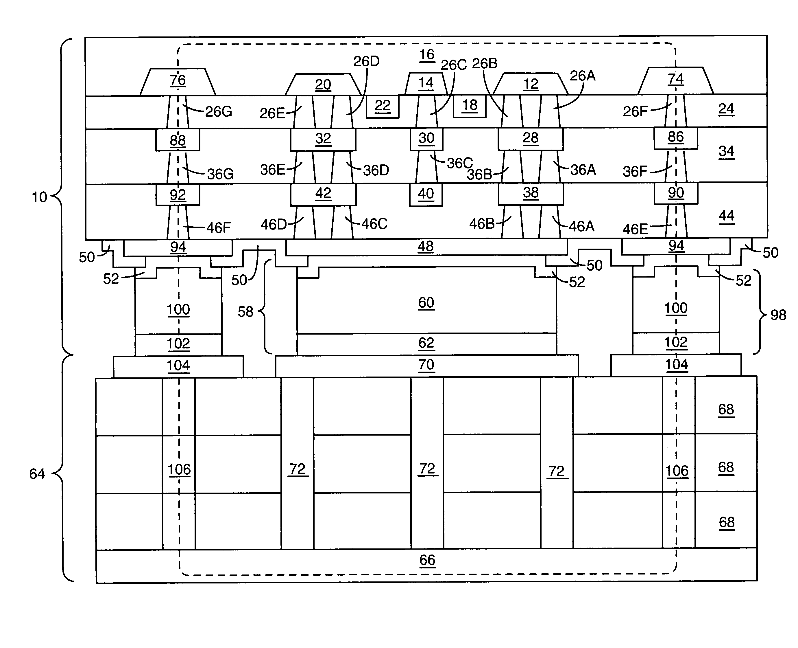
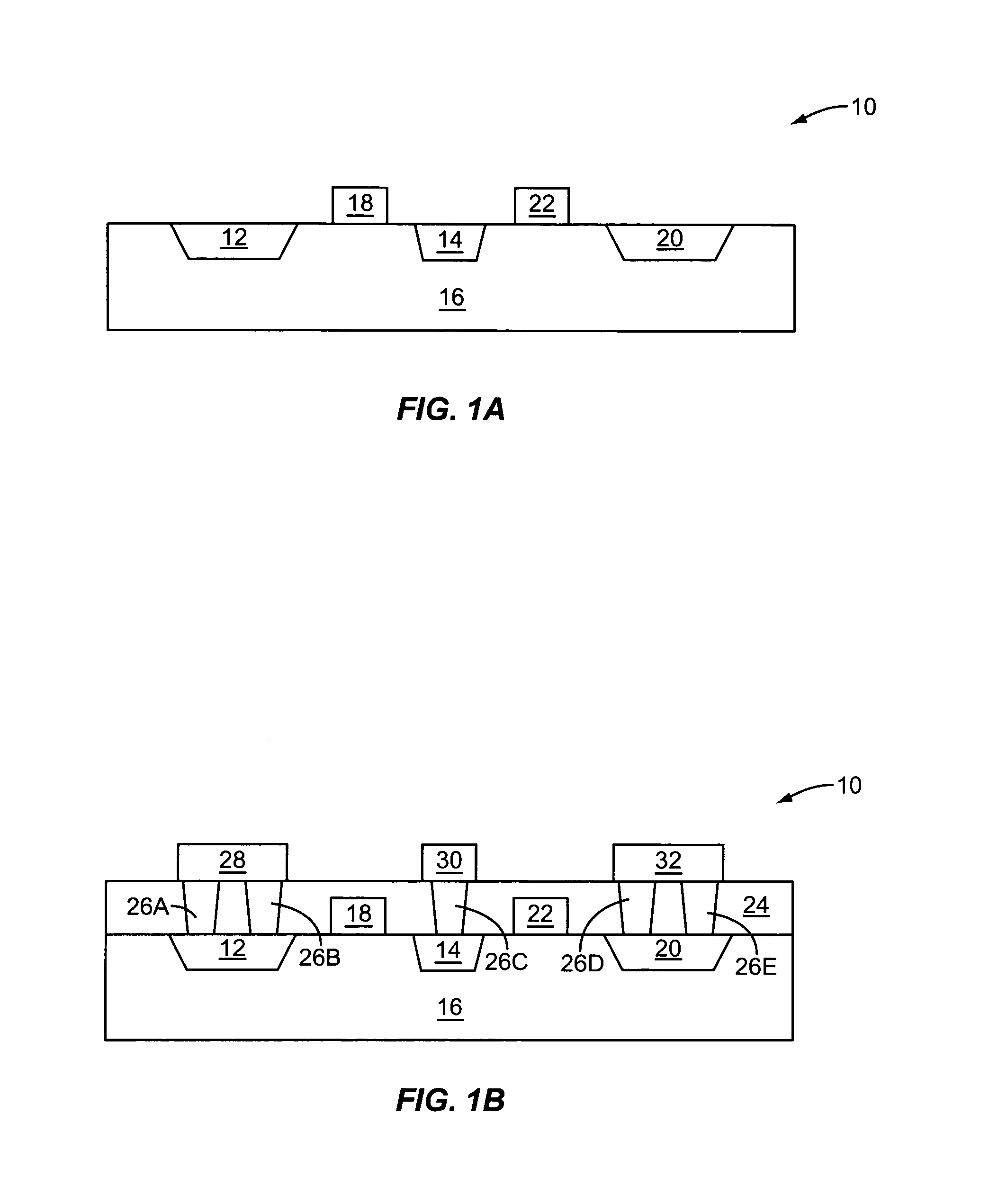
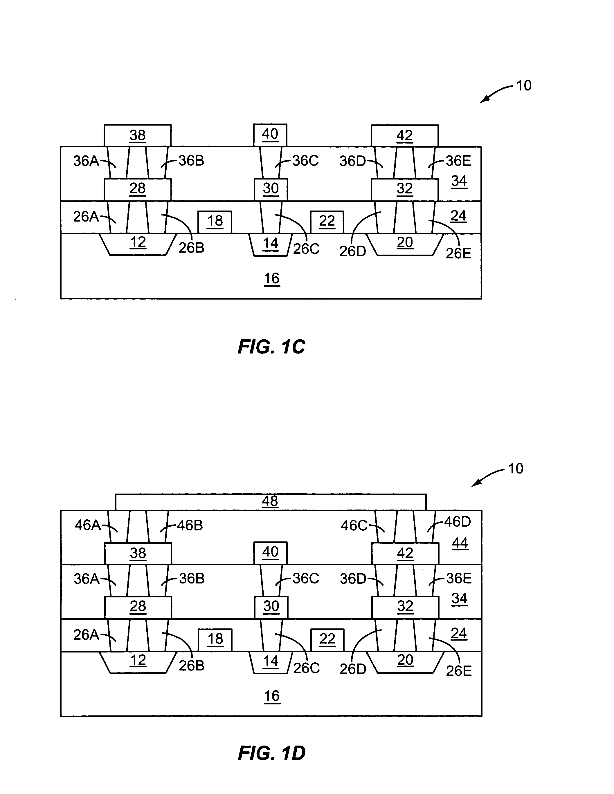
[0011]FIGS. 1A–1G illustrate a power device 10 at various states in a simplified fabrication process. As illustrated in FIG. 1A, the power device 10 includes first and second transistors. As described herein, the first and second transistors are Field Effect Transistors (FETs). However, it should be noted that the transistors may be alternatively be Bipolar Junction Transistors (BJTs) or any other type of transistor, as will be ap...


PUM


Abstract

A flip chip power device having an integrated low inductance ground and heat sink path and an isolation structure is provided. A substrate is formed having transistors and an ohmic contact region circumscribing the transistors. Dielectric layers are formed on the substrate, and a common metal layer is formed on the dielectric layers. An isolation metal layer is formed on the dielectric layers above the ohmic contact region. The common metal layer is coupled to a first region of each of the transistors, and the isolation metal layer is coupled to the ohmic contact region. A first bump is formed on the common metal layer, and a second bump is formed on the isolation metal layer. When the power device is attached to a second substrate, the first bump forms a low inductance ground and heat sink path to the second substrate, and an isolation structure is formed.

Description

FIELD OF THE INVENTION[0001]The present invention relates to an integrated power device and isolation structure formed using flip chip technology and providing both isolation from external noise and a low inductance ground and integrated heat sink path.BACKGROUND OF THE INVENTION[0002]Typically, power amplifiers and digital components for mobile terminals are fabricated as separate modules. As the desire for integrated devices continues to grow, a need has arisen for a power amplifier device capable of integration with digital circuitry on a single semiconductor die. Integration of a power amplifier requires a low inductance ground to have increased gain at high frequencies, heat conduction from the substrate to the environment, and isolation from nearby digital components. For a conventional silicon substrate, a low resistivity (typically less than 0.1 Ohm-cm) wafer is used along with high temperature thermal drives of high dose implants and is subsequently thinned for better therm...

Claims


Application Information

Patent Timeline
Patent Type & Authority Patents(United States)
IPC IPC(8): H01L23/12H01L23/053
CPCH01L23/3677H01L23/50H01L24/13H01L23/5286H01L23/66H01L24/10H01L2924/1305H01L2224/16235H01L2924/1306H01L2924/014H01L2223/6622H01L2224/13099H01L2224/16H01L2924/01015H01L2924/01029H01L2924/01074H01L2924/30107H01L2924/3025H01L2924/01033H01L2924/00H01L24/03H01L24/05H01L24/14H01L24/16H01L2224/05001H01L2224/05022H01L2224/05572H01L2224/056H01L2224/0603H01L2224/13H01L2924/00014H01L2224/05099
Inventor COSTA, JULIOIVANOV, TONYCARROLL, MICHAEL
Owner QORVO US INC
Why Eureka
Try Eureka