PN diode optical modulators fabricated in strip loaded waveguides

a technology of optical modulators and waveguides, applied in the field of optical modulators, can solve the problems of inherently difficult control of processes and inconsistent operation of lateral pn diodes, and achieve the effects of less impact on pn diodes, reduced production costs, and improved control

Active Publication Date: 2006-11-14
CISCO TECH INC
View PDF5 Cites 78 Cited by
  • Summary
  • Abstract
  • Description
  • Claims
  • Application Information

AI Technical Summary

Benefits of technology

[0007]High speed optical modulators can be made of a lateral PN diode formed in a strip loaded optical waveguide on a SOI or other silicon based substrate. A PN junction is formed at the boundary of the P and N doped regions. The depletion region at the PN junction overlaps with the center of a guided optical mode propagating through the waveguide. Electrically modulating a lateral PN diode causes a phase shift in an optical wave propagating through the waveguide. Due to differences in fabrication methods, forming strip loaded waveguides with consistent properties for use in PN diode optical modulators is much easier than fabricating similar rib waveguides. Forming the rib portion of a waveguide is typically done with a timed etch process and such a process is inherently difficult to control. Irregularities in the formation of a rib with doped sections can lead to the inconsistent operation of a late

Problems solved by technology

Forming the rib portion of a waveguide is typically done with a timed etch process and such a process is inherently difficult to control.
Irregularities in the formation of a rib with doped sections can lead to the inconsistent operation of a lateral PN diode form

Method used


Image

  • PN diode optical modulators fabricated in strip loaded waveguides
  • PN diode optical modulators fabricated in strip loaded waveguides
  • PN diode optical modulators fabricated in strip loaded waveguides

Examples


Embodiment Construction

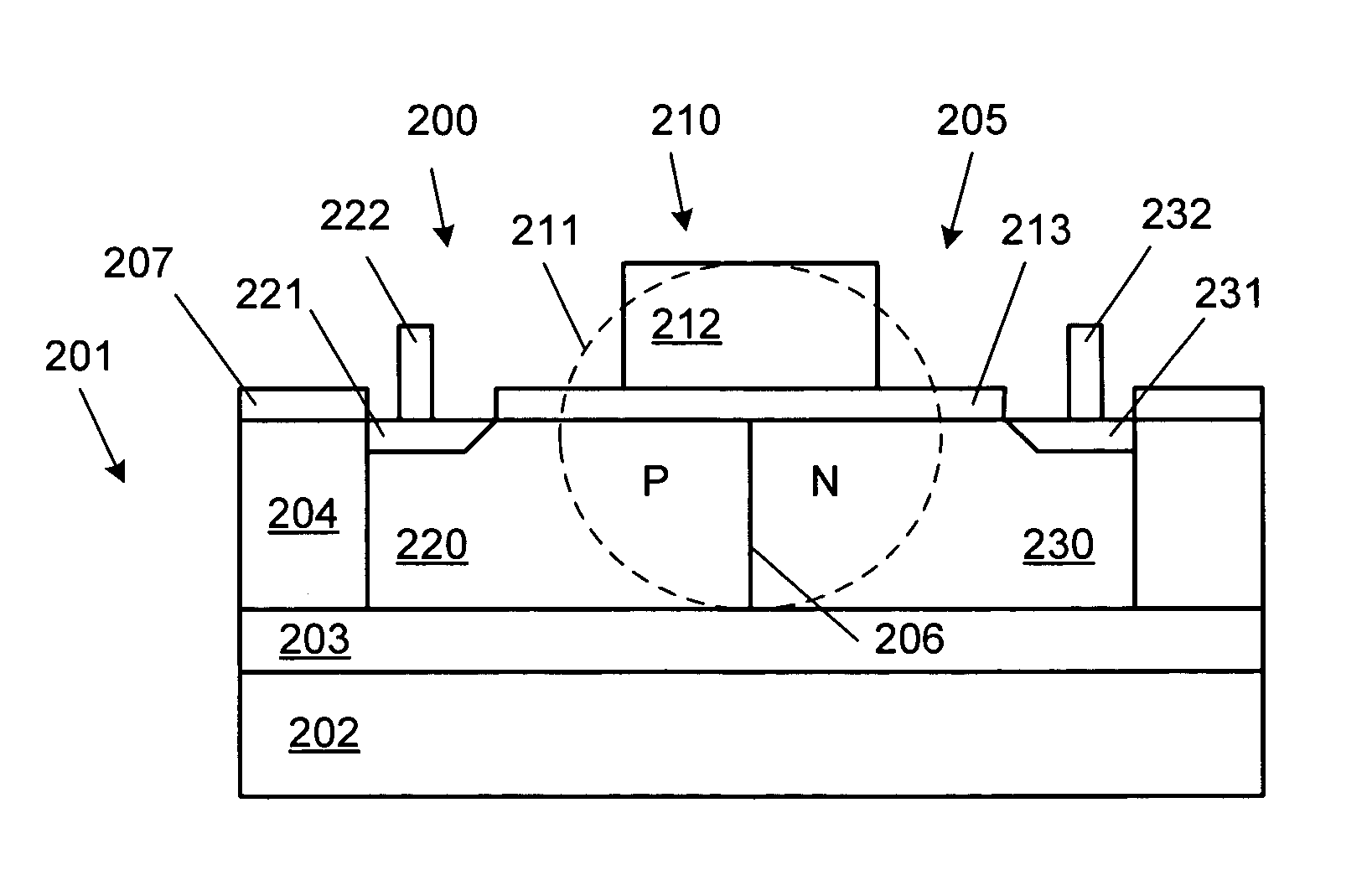
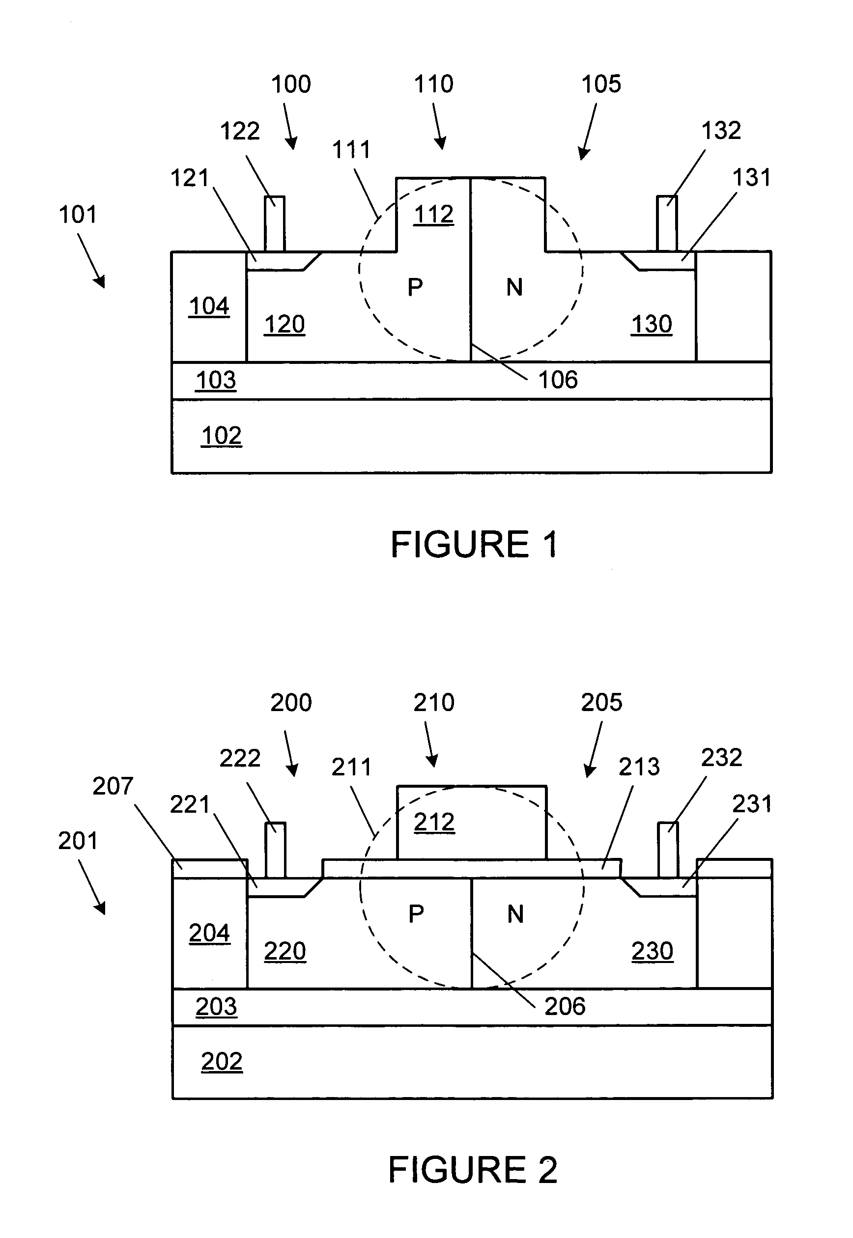
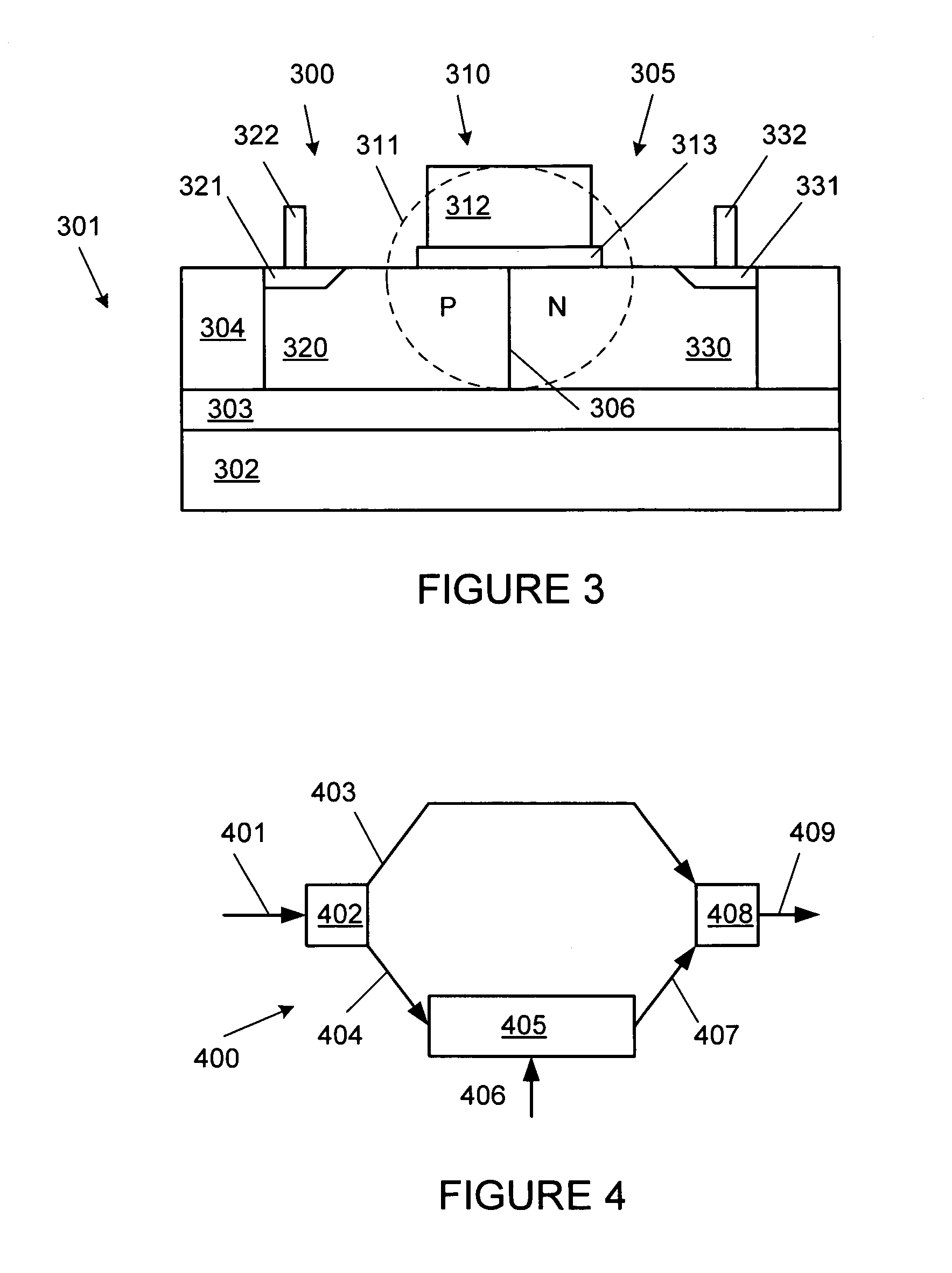
[0020]FIG. 1 is a cross sectional diagram, not to scale, of an integrated optical modulator, according to one embodiment of the present invention. Optical modulator 100 is made of lateral PN diode 105 fabricated across waveguide 110 on substrate 101. Substrate 11 in an exemplary embodiment is a SOI (silicon on insulator) substrate, made of silicon layer 104 on top of silicon dioxide layer 103, which is on top of silicon layer 102. Other types of substrates can be used, such as a five layer substrate made of three layers of silicon with two layers of silicon dioxide separating the silicon layers.

[0021]Waveguide 110 includes layer 104 and rib 112. Silicon layer 104 and rib 112 can be formed at the same time and of the same silicon used to form the silicon body of a transistor, such as a CMOS transistor. Vertical confinement of the optical wave is provided by the index contrast between silicon layer 104 and silicon dioxide layer 103 and a top level dielectric on top of waveguide 110. F...


PUM


Abstract

High speed optical modulators can be made of a lateral PN diode formed in a strip loaded optical waveguide on a SOI or other silicon based substrate. A PN junction is formed at the boundary of the P and N doped regions. The depletion region at the PN junction overlaps with the center of a guided optical mode propagating through the waveguide. Electrically modulating a lateral PN diode causes a phase shift in an optical wave propagating through the waveguide. Due to differences in fabrication methods, forming strip loaded waveguides with consistent properties for use in PN diode optical modulators is much easier than fabricating similar rib waveguides.

Description

CROSS-REFERENCE TO RELATED APPLICATIONS[0001]This application claims priority from U.S. Provisional applications No. 60 / 495,402, No. 60 / 495,403 and No. 60 / 495,404 filed Aug. 15, 2003. This application is related to copending U.S. patent applications entitled: “PN Diode Optical Modulators Fabricated In Rib Waveguides,”“PN Diode Optical Modulators With Variegated PN Junctions” and “Doping Profiles In PN Diode Optical Modulators,” which are to be filed on the same date as this application.FIELD OF THE INVENTION[0002]The present invention relates to optical modulators for use in optoelectronic integrated circuits.BACKGROUND OF THE INVENTION[0003]Optical fibers have been widely used for the propagation of optical signals, especially to provide high speed communications links. Optical links using fiber optics have many advantages compared to electrical links: large bandwidth, high noise immunity, reduced power dissipation and minimal crosstalk. Fiber optic communications links can operate...

Claims


Application Information

Patent Timeline
IPC IPC(8): G02F1/025G02B6/10
CPCG02B6/12004G02B6/122G02F1/025
Inventor GUNN, III, LAWRENCE C.KOUMANS, ROGERLI, BINGLI, GUO LIANGPINGUET, THIERRY J.
Owner CISCO TECH INC
Why Eureka
Try Eureka