Organic electroluminescent devices having a stability-enhancing layer
a technology of stability-enhancing layer and electroluminescent device, which is applied in the direction of discharge tube luminescnet screen, natural mineral layered product, etc., can solve the problems of diffusive report and luminescence quenching in oleds, and achieve the effect of increasing operational stability and reducing drive voltag
- Summary
- Abstract
- Description
- Claims
- Application Information
AI Technical Summary
Benefits of technology
Problems solved by technology
Method used
Image
Examples
example 1
Comparative Example
[0118]The preparation of a conventional OLED is as follows: A˜1.1 mm thick glass substrate coated with a transparent ITO conductive layer was cleaned and dried using a commercial glass scrubber tool. The thickness of ITO is about 42 nm and the sheet resistance of the ITO is about 68 Ω / square. The ITO surface was subsequently treated with oxidative plasma to condition the surface as an anode. A layer of CFx, 1 nm thick, was deposited on the clean ITO surface as the HIL by decomposing CHF3 gas in an RF plasma treatment chamber. The substrate was then transferred into a vacuum deposition chamber (TROVATO MFG. INC) for deposition of all other layers on top of the substrate. All organic materials were sublimed before use. The following layers were deposited in the following sequence by evaporation from a heated boat under a vacuum of approximately 10−6 Torr:[0119](1) a HTL, 90 nm thick, consisting of NPB;[0120](2) a LEL, 20 nm thick, consisting of TBADN doped with 1.5%...
example 2
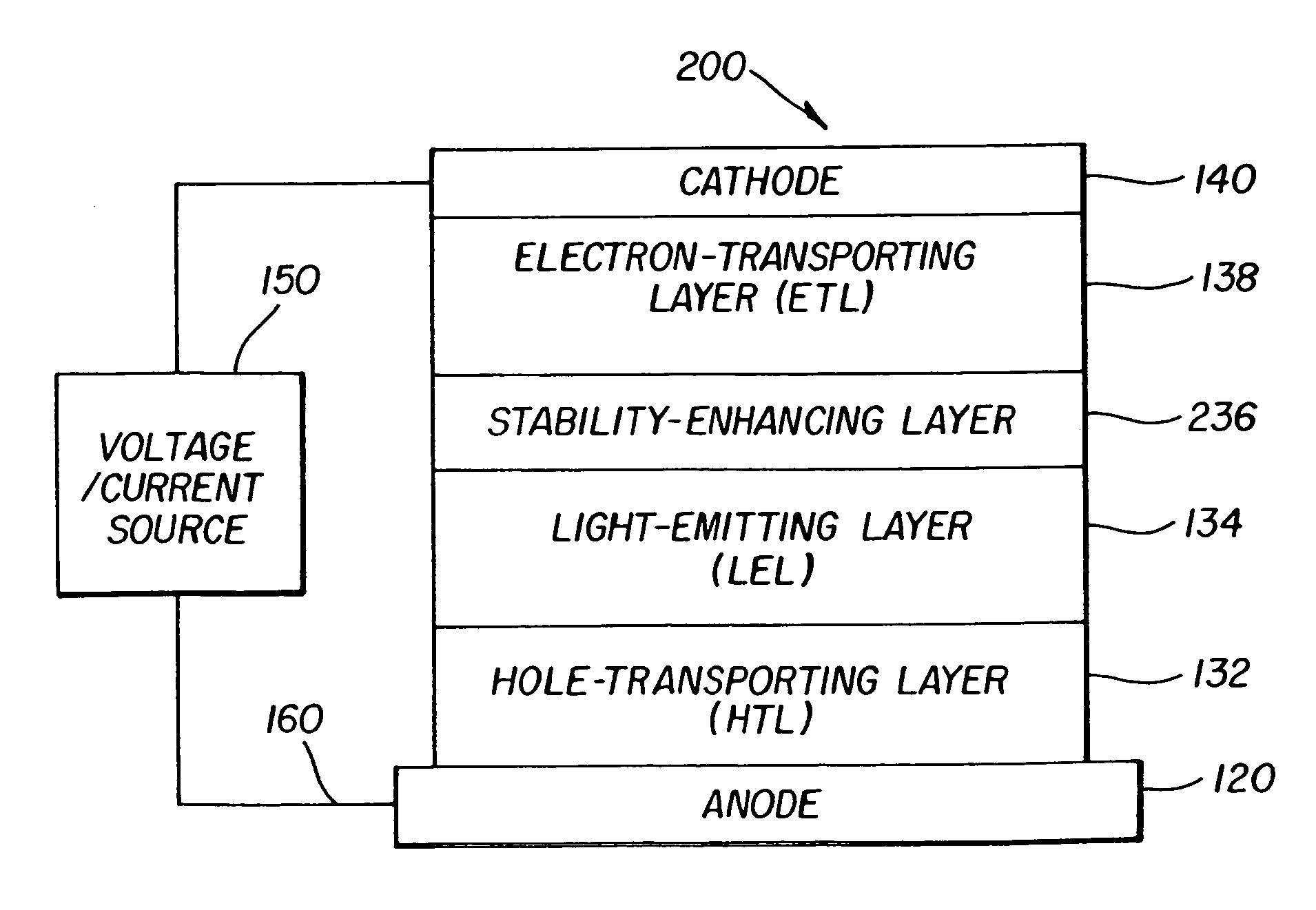
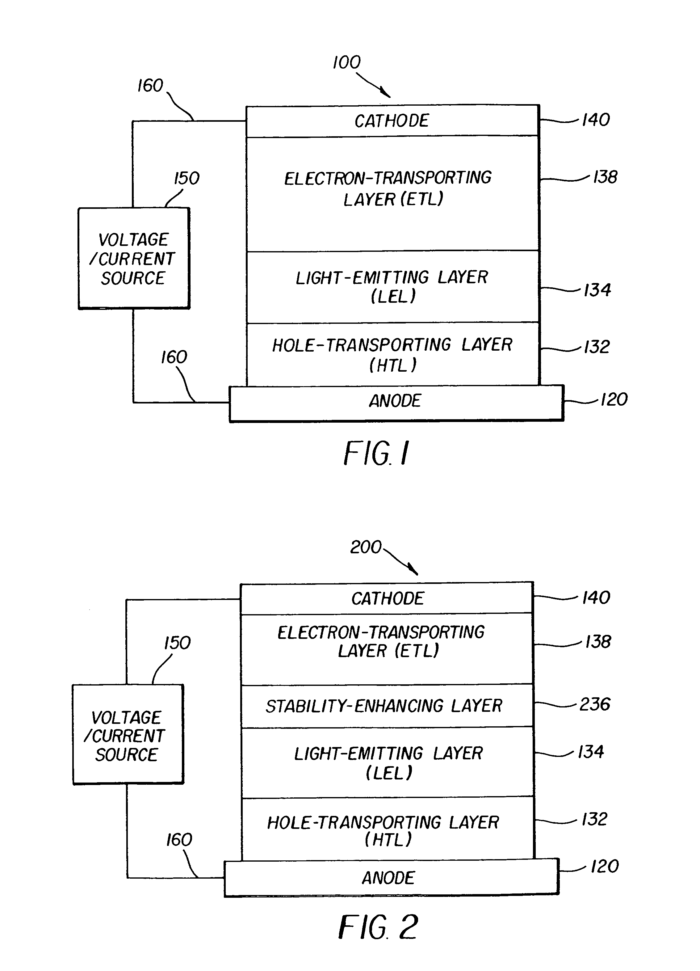
[0124]An OLED was constructed in the manner described in Example 1, except that one more layer was added onto the LEL. The layers were deposited in the following sequence:[0125](1) a HTL, 90 nm thick, consisting of NPB;[0126](2) a LEL, 20 nm thick, consisting of TBADN doped with 1.5% TBP by volume;[0127](3) a stability-enhancing layer, 2.5 nm thick, consisting of Alq doped with 1.2% Li by volume;[0128](4) an ETL, 32.5 nm thick, consisting of Alq; and[0129](5) a cathode, approximately 210 nm thick, consisting of MgAg.
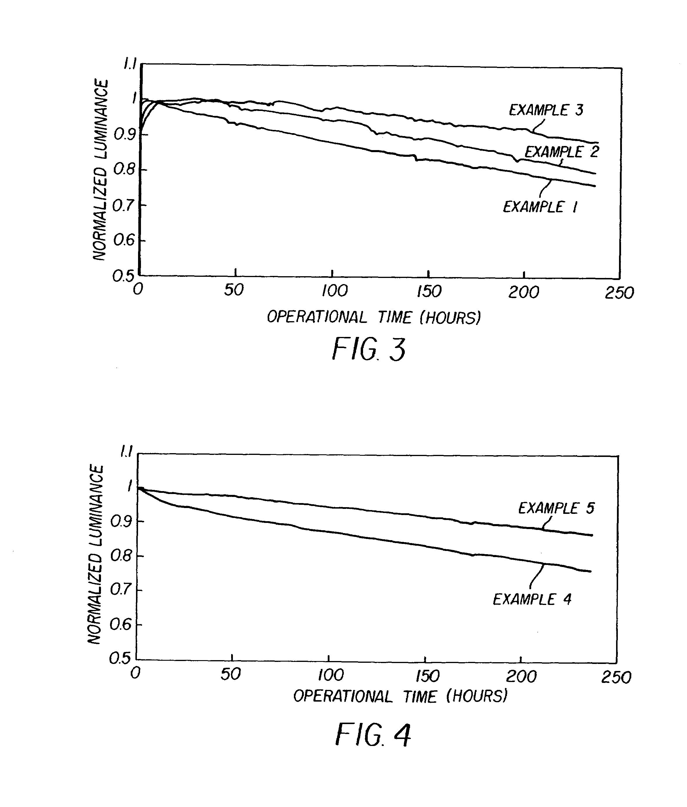
[0130]The completed device structure is denoted as ITO / CFx / NPB(90) / TBADN:TBP(1.5%)(20) / Alq:Li(1.2%)(2.5) / Alq(32.5) / MgAg. The EL performance of the device, measured at a current density of 20 mA / cm2, is shown in Table I, wherein the drive voltage, luminance, luminous efficiency, power efficiency, color coordinates CIEx,y, and the T90(70° C.) are listed. The normalized luminance vs. operational time is shown in FIG. 3.
example 3
[0131]An OLED was constructed in the manner described in Example 2, except in Step (3) wherein the thickness of the stability-enhancing layer is now increased to 15 nm, and except in Step (4) wherein the thickness of the ETL is now reduced to 20 nm. The completed device structure is denoted as ITO / CFx / NPB(90) / TBADN:TBP(1.5%)(20) / Alq:Li(1.2%)(1.5) / Alq(20) / MgAg. The EL performance of the device, measured at a current density of 20 mA / cm2, is shown in Table I, wherein the drive voltage, luminance, luminous efficiency, power efficiency, color coordinates CIEx,y, and the T90(70° C.) are listed. The normalized luminance vs. operational time is shown in FIG. 3.
[0132]
TABLE IExample (Type)LuminousPower(EL measuredVoltageLuminanceEfficiencyEfficiencyT90 (70° C.)@ 20 mA / cm2)(V)(cd / m2)(cd / A)(lm / W)CIEyCIEy(Hrs)1 (Comparative)8.494222.110.780.1420.213842 (Inventive)9.043901.950.680.1340.1941353 (Inventive)8.323741.870.710.1340.202218
[0133]From the data shown in both Table I and FIG. 3, we find th...
PUM
| Property | Measurement | Unit |
|---|---|---|
| thickness | aaaaa | aaaaa |
| thickness | aaaaa | aaaaa |
| thickness | aaaaa | aaaaa |
Abstract
Description
Claims
Application Information


