Element substrate and light emitting device

a technology of element substrate and light emitting device, which is applied in the direction of static indicating device, instruments, transistors, etc., can solve the problems of affecting the image quality of the device, and the characteristic variation is likely to be increased, so as to enhance the image quality, increase the storage capacity of the capacitor, and reduce the effect of the cause of variation

Inactive Publication Date: 2006-11-28
SEMICON ENERGY LAB CO LTD
View PDF19 Cites 37 Cited by
  • Summary
  • Abstract
  • Description
  • Claims
  • Application Information

AI Technical Summary

Benefits of technology

[0019]Current flowing in the light emitting element is not influenced even without increasing storage capacity of a capacitor which is disposed between the gate and source of the current controlling transistor or suppressing off-current of the switching transistor low. In addition, it is not influenced by the parasitic capacitance on the gate of the current controlling transistor either. Therefore, cause of variation is decreased, and image quality is thus enhanced to a great extent.
[0020]In addition, as there is no need to suppress off-current of the switching transistor low, manufacturing process of the transistor can be simplified, thus contributes greatly to the cost reduction and improvement in yield.

Problems solved by technology

However, the transistor using polysilicon has problems in that it is likely to have variations in characteristics due to a defect in a crystal grain boundary.

Method used


Image

  • Element substrate and light emitting device
  • Element substrate and light emitting device
  • Element substrate and light emitting device

Examples


embodiment mode 1

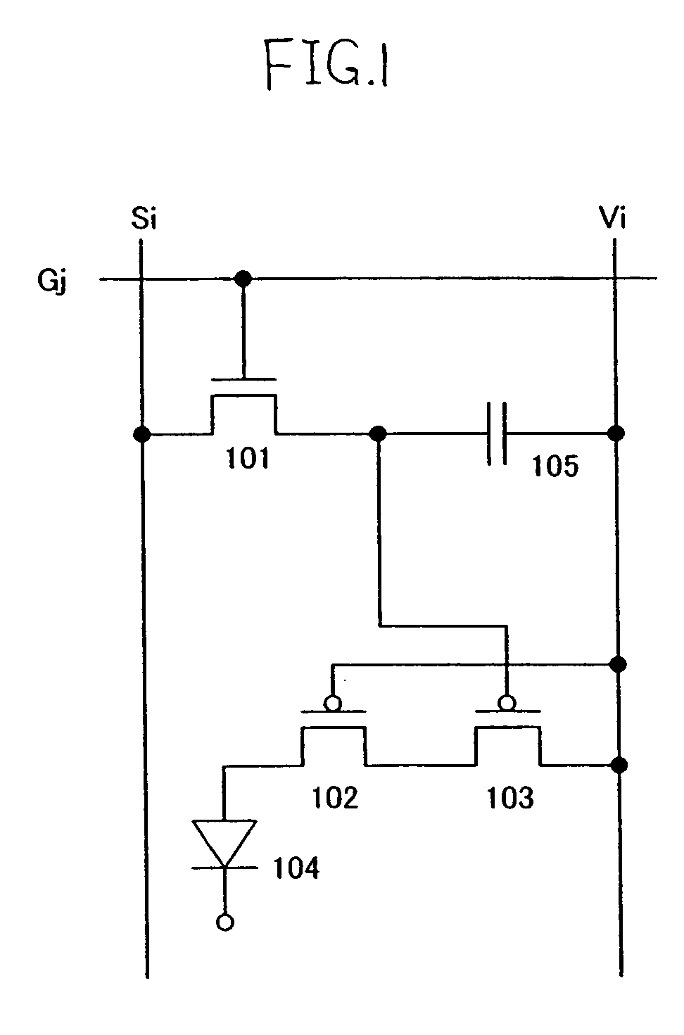
[0034]FIG. 1 shows an embodiment mode of a pixel of the light emitting device of the invention. The pixel shown in FIG. 1 comprises a light emitting element 104, a transistor (switching transistor) 101 used as a switching element for controlling an input of a video signal to the pixel, a driving transistor 102 for controlling current flowing in the light emitting element 104, and a current controlling transistor 103 for controlling a current supply to the light emitting element 104. In addition, it is also possible to dispose in the pixel a capacitor 105 for storing a potential of a video signal.

[0035]The driving transistor 102 and the current controlling transistor 103 have the same conductivity. It is assumed that the driving transistor 102 is a depletion mode transistor, and the rest of the transistors are normal enhancement mode transistors. In the invention, the driving transistor 102 is operated in a saturation region and the current controlling transistor 103 is operated in a...

embodiment mode 2

[0049]Described in this embodiment mode is a different configuration of a pixel of the light emitting device from that shown in FIG. 1.

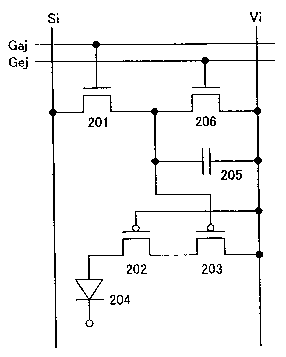
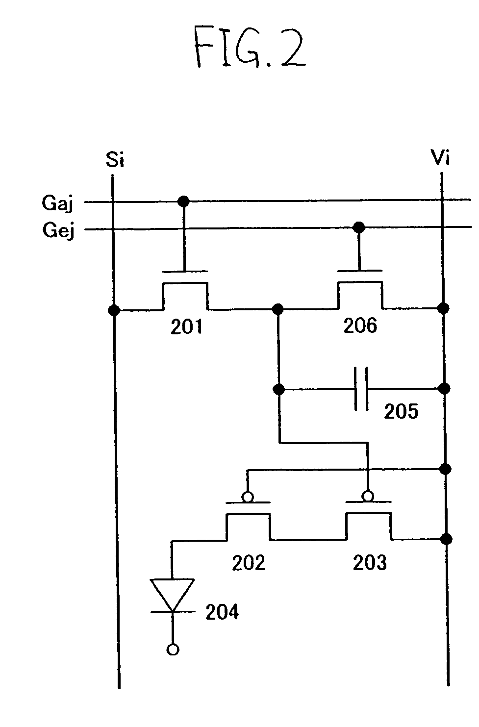
[0050]The pixel shown in FIG. 2 comprises a light emitting element 204, a switching transistor 201, a driving transistor 202, a current controlling transistor 203, and a transistor (erasing transistor) 206 for turning OFF the current controlling transistor 203 forcibly. In addition, it is also possible to dispose a capacitor 205 in addition to the aforementioned elements.

[0051]The driving transistor 202 and the current controlling transistor 203 have the same conductivity. The size, characteristics, and operating region of each transistor may be set in the same manner as Embodiment Mode 1.

[0052]The gate of the switching transistor 201 is connected to a first scan line Gaj (j=1 to y). Either the source or drain of the switching transistor 201 is connected to a signal line Si (i=1to x), and the other is connected to the gate of the current controlling ...

embodiment mode 3

[0059]Described in this embodiment mode is a different configuration of a pixel of the light emitting device of the invention from those of Embodiment Modes 1 and 2.

[0060]The pixel shown in FIG. 3 comprises a light emitting element 304, a transistor (switching transistor) 301 used as a switching element for controlling input of a video signal to the pixel, a driving transistor 302 for controlling a current flowing into the light emitting element 304, a current controlling transistor 303 for controlling a current supply to the light emitting element 304. In addition, it is also possible to dispose a capacitor 305 for storing a potential of a video signal as shown in the figure.

[0061]The driving transistor 302 and the current controlling transistor 303 have the same conductivity. The size, characteristics, and operating region of each transistor may be set in the same manner as those of Embodiment Mode 1.

[0062]The gate of the switching transistor 301 is connected to a scan line Gj (j=...


PUM


Abstract

A light emitting device and an element substrate which are capable of suppressing variations in the luminance intensity of a light emitting element among pixels due to characteristic variations of a driving transistor without suppressing off-current of a switching transistor low and increasing storage capacity of a capacitor. According to the invention, a depletion mode transistor is used as a driving transistor. The gate of the driving transistor is fixed in its potential or connected to the source or drain thereof to operate in a saturation region with a constant current flow. A current controlling transistor which operates in a linear region is connected in series to the driving transistor, and a video signal for transmitting a light emission or non-emission of a pixel is inputted to the gate of the current controlling transistor through a switching transistor.

Description

BACKGROUND OF THE INVENTION[0001]1. Field of the Invention[0002]The present invention relates to a light emitting device comprising a plurality of pixels each having a light emitting element and a means for supplying current to the light emitting element.[0003]2. Description of the Related Art[0004]Since a light emitting element emits light by itself, it is highly visible and does not require a back light which is needed in a liquid crystal display device (LCD). Therefore, it is suitably applied to thin devices and not restricted in viewing angle. Because of these advantages, a light emitting device having a light emitting element has recently been drawing attentions as an alternative display device to a CRT and an LCD. It is to be noted that a light emitting element in this specification indicates an element whose luminance is controlled by current or voltage, and it includes an OLED (Organic Light Emitting Diode) or an MIM electron source element (electron discharge element) and t...

Claims


Application Information

Patent Timeline
Patent Type & Authority Patents(United States)
IPC IPC(8): G09G5/00H01L51/50G09G3/20G09G3/30G09G3/32H01L29/786H05B33/14H05B37/00H05B37/02
CPCG09G3/3233H01L27/283H01L51/5296H01L27/326H01L29/78672H01L51/5012G09G3/2022G09G2300/0417G09G2300/0842G09G2300/0885G09G2310/0251H10K59/121H10K19/10H10K50/11H10K50/30
Inventor OSAME, MITSUAKIANZAI, AYAYAMAZAKI, YU
Owner SEMICON ENERGY LAB CO LTD
Why Eureka
Try Eureka