Method and apparatus for detecting defects

a technology of defect detection and method, applied in the field of high-resolution optical systems, can solve the problems of difficult to distinguish grain from other defects, difficult to detect certain defects such as residual thin films, and small unevenness on the surface of metal wiring

Inactive Publication Date: 2006-11-28
HITACHI LTD
View PDF10 Cites 21 Cited by
  • Summary
  • Abstract
  • Description
  • Claims
  • Application Information

AI Technical Summary

Benefits of technology

[0004]According to an object of the present invention, it is possible to implement more

Problems solved by technology

However, for example, in the dark field illumination mode, it may be difficult to detect certain defects such as residual thin films, if any.
Further, when semiconductor devices are inspected, minute unevenness (grains) may be appeared on a surface of metal wiring created in a

Method used


Image

  • Method and apparatus for detecting defects
  • Method and apparatus for detecting defects
  • Method and apparatus for detecting defects

Examples


Embodiment Construction

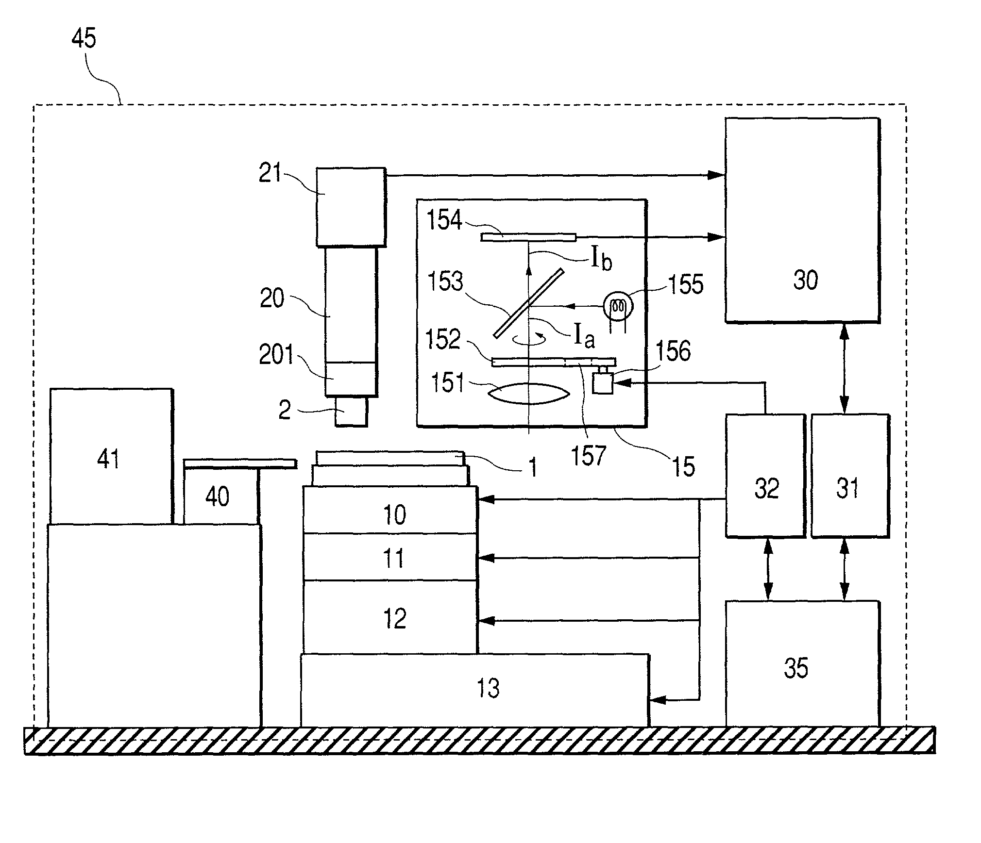
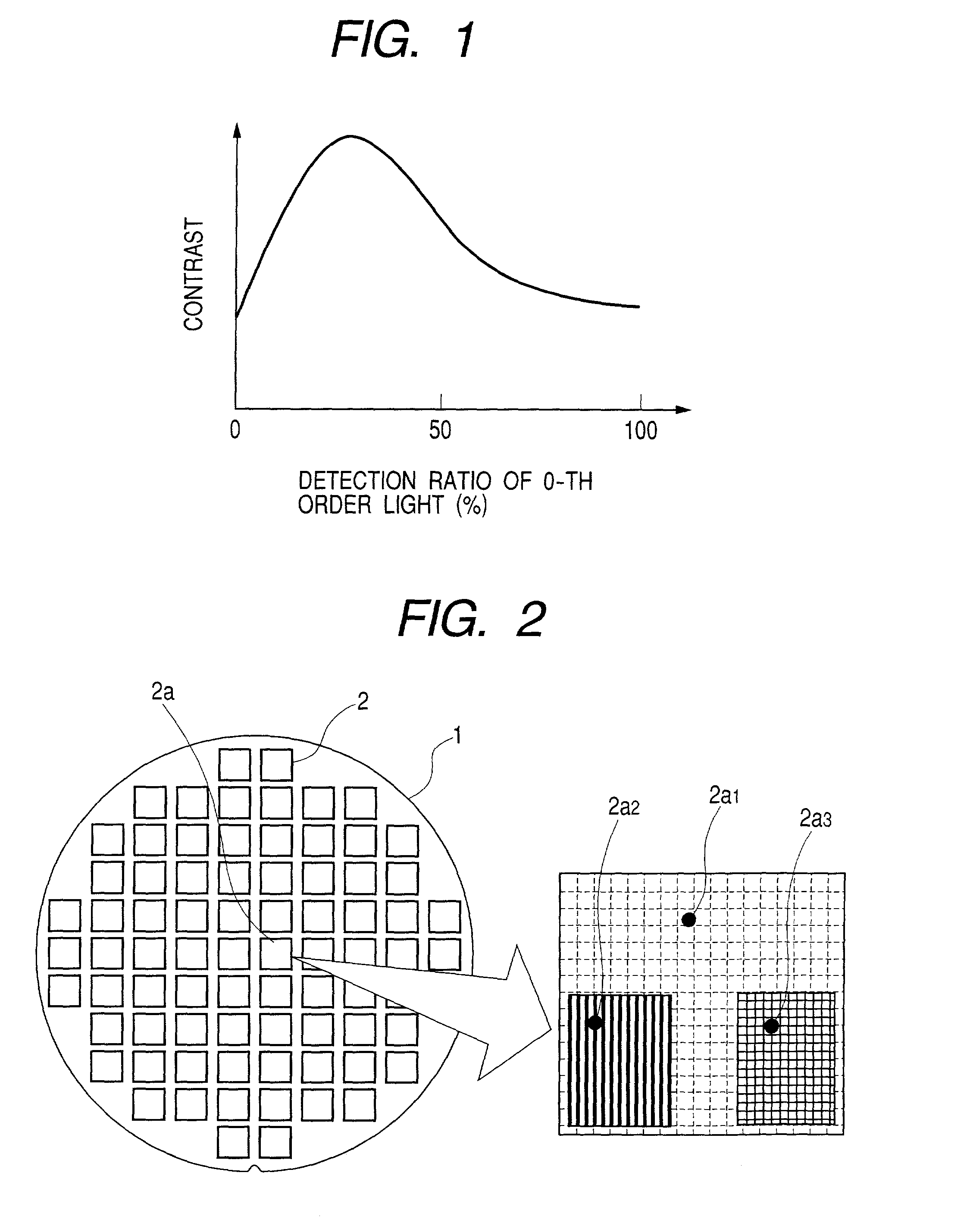
[0022]An embodiment of the present invention is shown in FIG. 5. A sample (a wafer) 1 contained in a cassette 41 is transported to a Z-stage 10, a θ-stage 11, an X-stage 12 and a Y-stage 13 by a wafer transporting robot 40 of the system 45. The wafer 1 that has been transported to any one of the stages is moved into a field of view of a sub-optical system 20 having low magnification for detection in an entire chip area to detect an image of the entire chip area. Then, the chip image being divided into a peripheral circuit 2a1, a logic part 2a2, a memory part 2a3 and the like, is captured by a camera 21 in the sub-optical system 20. This image is transferred to an image processing section 30. This image is stored in a data server 31. The system is configured so that this image may be shown on a display of an operating computer 35 in this inspection apparatus. Therefore, the operating computer 35 can select a region (a peripheral circuit part 2a1, a logic part 2a2, a memory part 2a3 a...


PUM


Abstract

An image of a sample that has high contrast both in large and fine pattern parts is acquired by using an optical system for coaxial bright field epi-illumination, forming the optical image of the sample with various transmission ratio of 0-th order diffracted light that is reflected regularly from the sample, and capturing the image by an image sensor. Optical conditioning is automatically set and in a short time by detecting a plurality of optical images of the sample under various conditions for the transmission ratio of the 0-th order diffracted light, evaluating quality of the detected images, and determining the transmission ratio of the 0-th order diffracted light showing the maximum defect detection sensitivity.

Description

BACKGROUND OF THE INVENTION[0001]The present invention relates to a high resolution optical system for inspection and observation of fine pattern defects, foreign particles and the like that is typically performed in manufacturing process of semiconductors and flat panel displays and also relates to a method and an apparatus for detecting defects by using such optical system.[0002]As a prior art, Japanese Patent Laid-open No. Hei 8-327554 discloses a technique for improving contrast of an object by changing an impinging angle of illumination depending on optical characteristics of the object to be observed.[0003]In the above prior art, the impinging (incident) angle of the illumination is changed and determined so that minute unevenness on a surface of the object becomes obvious by improving the contrast of the unevenness. In such method, an optical system for oblique illumination and oblique detection is utilized, wherein the optical system changes a viewing mode of the object from...

Claims


Application Information

Patent Timeline
IPC IPC(8): G01N21/00G06K9/00G01N21/21G01N21/95
CPCG01N21/9501G01N21/21
Inventor SHIBATA, YUKIHIROMAEDA, SHUNJI
Owner HITACHI LTD
Why Eureka
Try Eureka