Defect detection method and its apparatus

a detection method and detection method technology, applied in image enhancement, semiconductor/solid-state device testing/measurement, instruments, etc., can solve problems such as reducing sensitivity, alignment at a wrong position, and misalignment of two images

Active Publication Date: 2006-11-28
HITACHI LTD
View PDF21 Cites 31 Cited by
  • Summary
  • Abstract
  • Description
  • Claims
  • Application Information

AI Technical Summary

Benefits of technology

[0014]In addition, a defect detection apparatus according to the present invention comprises a means for performing correction according to a contrast between an image to be inspected and a reference image so that a difference between the images is minimized. As an effective example, a defect detection apparatus according to the present invention comprises a defect inspecting means characterized in that, in a high-contrast part where even when the displacement is minute, a difference between the images becomes large, correction is performed beforehand so as to minimize the difference; and in final defect detection processing, a defect is detected using a specific low threshold value, that is to say, with high sensitivity, for all contrasts.
[0015]Moreover, a defect detection apparatus according to the present invention comprises a means for monitoring the accuracy of displacement, and thereby for performing correction, only when misalignment occurs, so as to minimize a difference between the images in a high-contrast part where displacement causes improper detection.
[0017]The means described above provide a defect detection method, and a defect detection apparatus, which can adjust sensitivity of all areas to be inspected using a single threshold value.

Problems solved by technology

However, in reality, there are the vibration of a stage and the inclination of a target, which may cause the positions of two images to become misaligned.
However, if the quantity of displacement is not correctly determined when the displacement is detected, the alignment will be performed at a wrong position.
This method decreases sensitivity, with the result that a defect having a difference value smaller than or equal to that of the edges cannot be detected.
This means that a plurality of threshold values has to be handled, leading to complicated adjustment of sensitivity.
This is also a false report.

Method used


Image

  • Defect detection method and its apparatus
  • Defect detection method and its apparatus
  • Defect detection method and its apparatus

Examples


Embodiment Construction

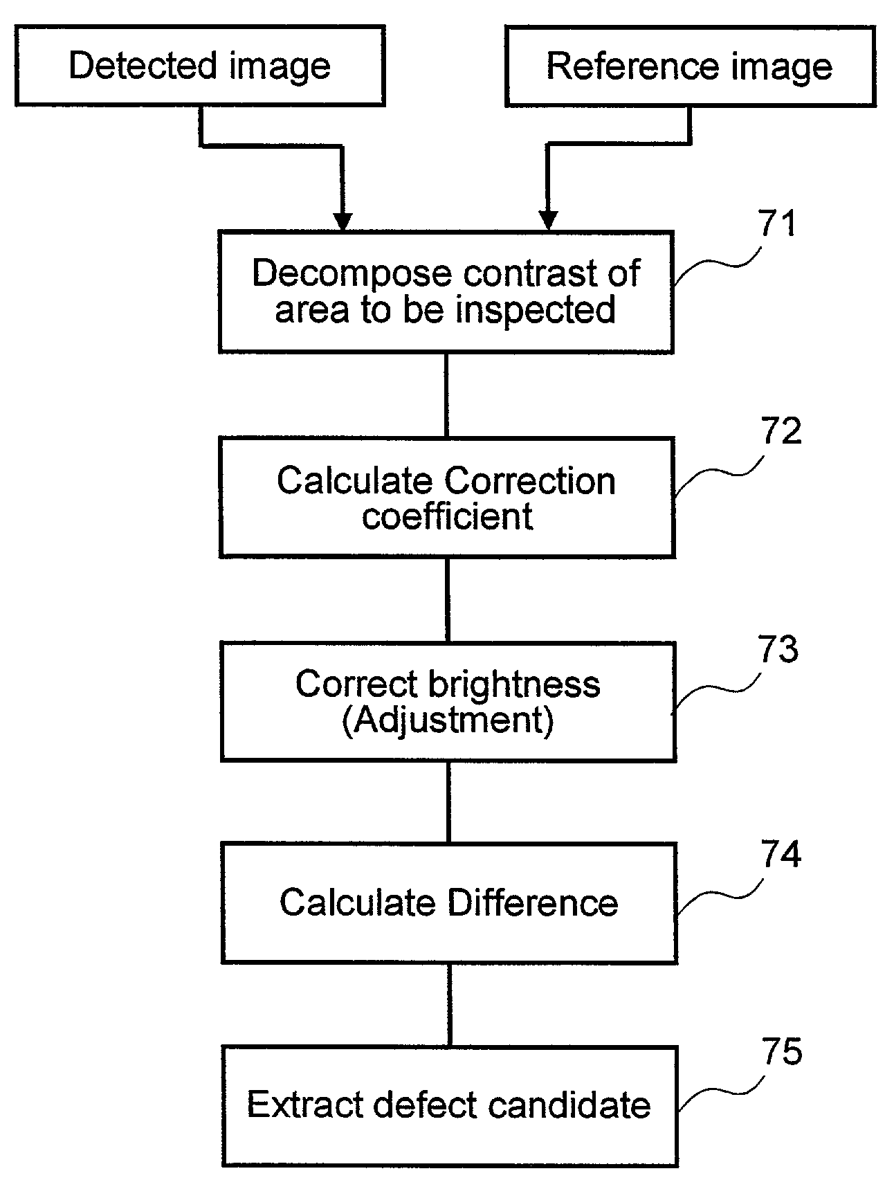
[0043]An embodiment of the present invention will be described in detail with reference to drawings below.

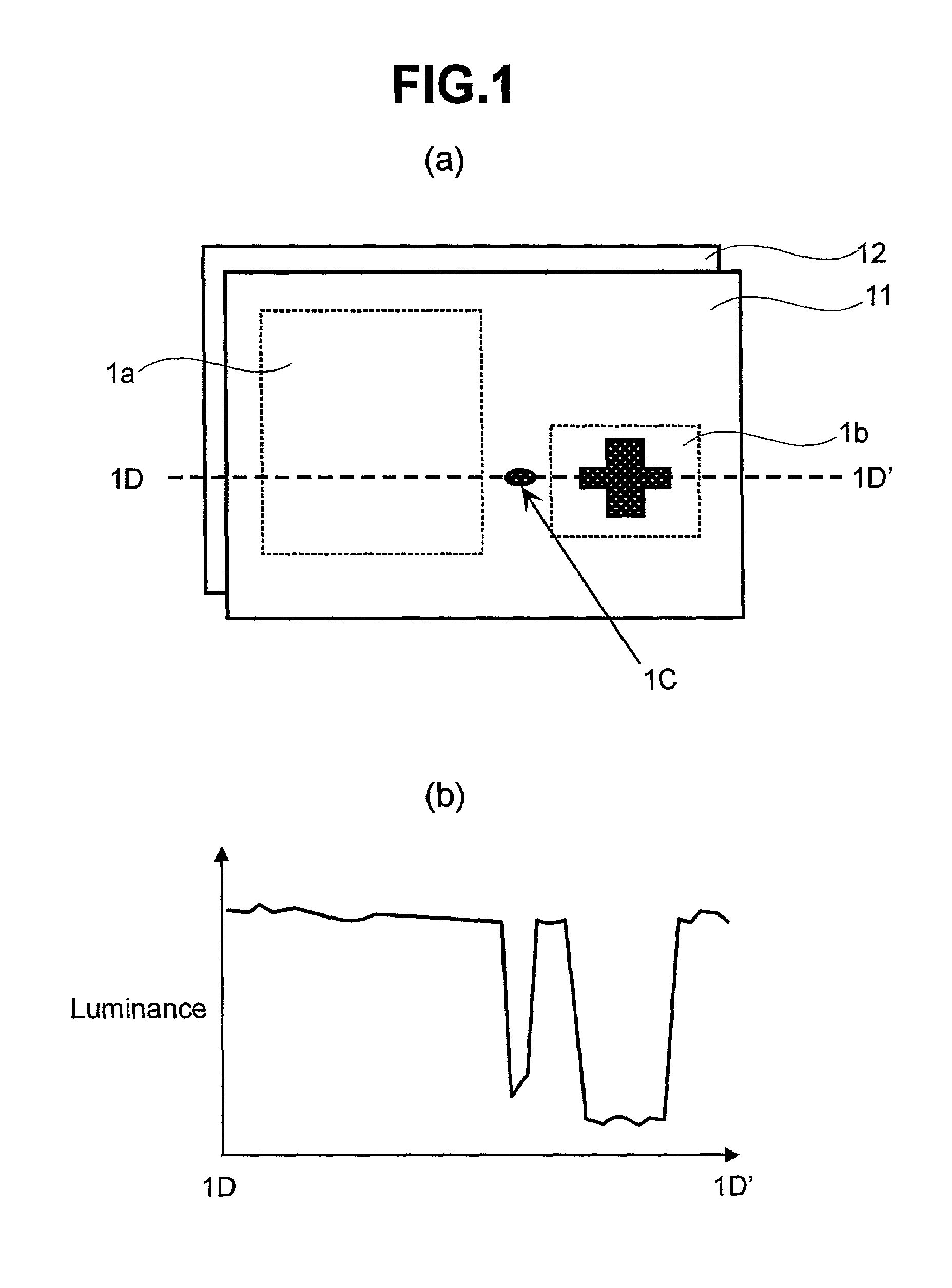
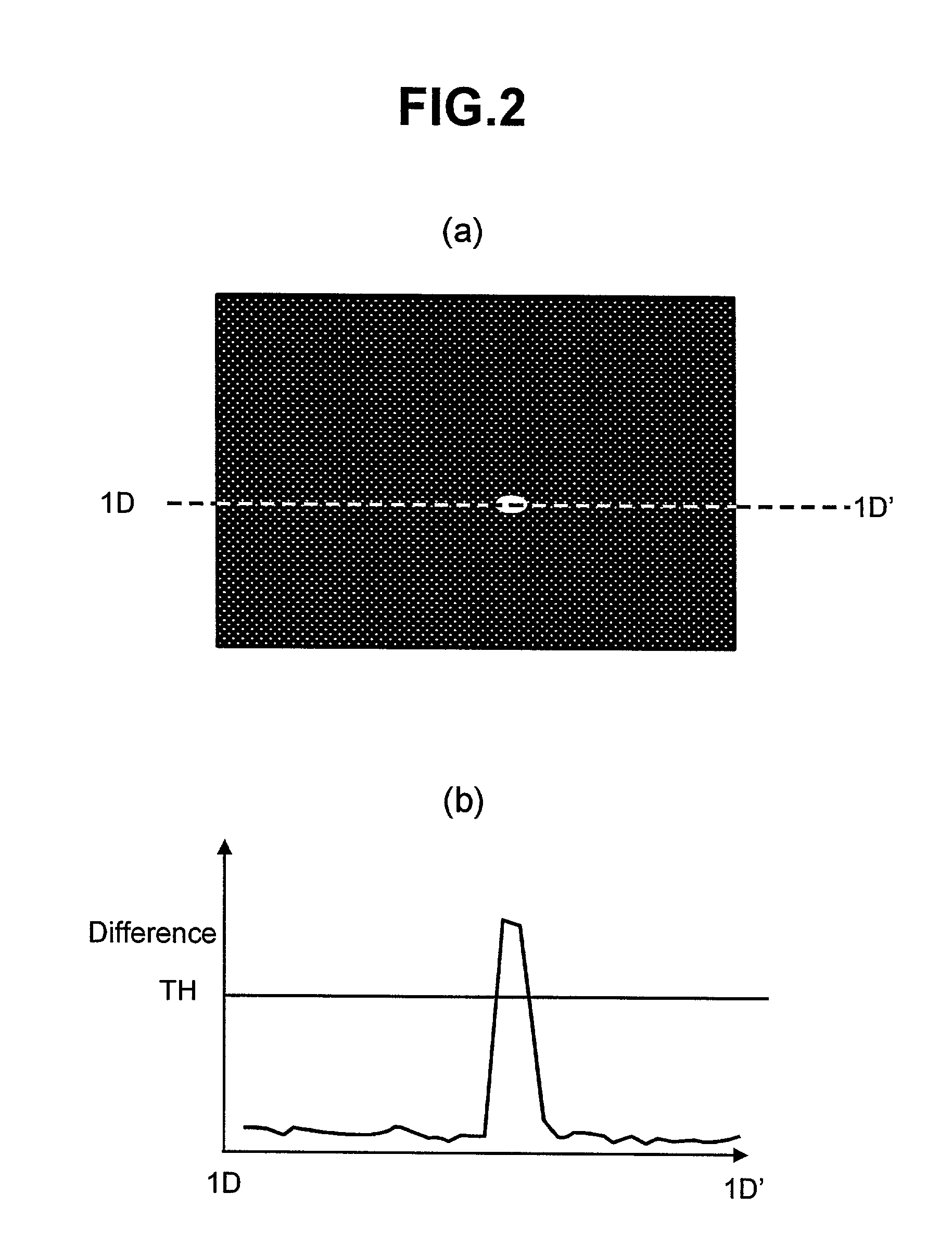
[0044]In this embodiment, a defect detection method of an optical visual inspecting apparatus targeted for a semiconductor wafer is taken as an example. FIG. 5 illustrates a configuration of the apparatus. Reference numeral 51 is a sample (an object to be inspected, such as a semiconductor wafer); reference numeral 52 is a stage on which the sample 51 is placed, and which can be moved at least in an XY plane; and reference numeral 53 is a detecting unit. The detecting unit 53 includes: a light source 501 for illuminating the sample 51; an illumination optical system 502 for condensing light emitted from the light source 501; an objective lens 503 through which the sample 51 is illuminated with illuminated light condensed in the illumination optical system 502, and through which an optical image obtained by reflection is formed; and an image sensor 504 for receiving the formed op...


PUM

PropertyMeasurementUnit
defect detectionaaaaaaaaaa
displacementaaaaaaaaaa
brightnessaaaaaaaaaa

Abstract

An object of the present invention is to provide a defect detection method and its apparatus which can adjust sensitivity easily by managing both reduction in the number of false reports and highly-sensitive detection of a defect using single threshold value setting in comparison inspection that compares an image to be inspected with a reference image to detect a defect judging from a difference between the images. According to the present invention, adjusting the brightness before inspection so that a difference becomes small at the edges of a high-contrast pattern in a target image enables reduction in the number of false reports caused by an alignment error, and achievement of highly-sensitive defect inspection using a low threshold value, without increasing the threshold value. Moreover, in the case of inspection targeted for a semiconductor wafer, which produces a problem of irregularity in brightness of a pattern caused by a difference between film thicknesses, the present invention reduces the number of false reports caused by the irregularity in brightness, and realizes inspection with high sensitivity without increasing a threshold value, by adjusting the brightness of both images before the inspection.

Description

BACKGROUND OF THE INVENTION[0001]The present invention relates to a defect detection method and an apparatus therefor in which an image of a target such as a semiconductor wafer, a TFT, and a photo mask, which is obtained using light or a laser beam, is compared with a reference image stored beforehand, and then a minute pattern defect, a foreign material, and the like are inspected judging from a difference obtained by the comparison. In particular, the present invention relates to a defect detection method and an apparatus therefor that are suitable for visual inspection of a semiconductor wafer.[0002]The prior art in which an image to be inspected is compared with a reference image so as to detect a defect is disclosed by Japanese Patent Laid-Open No. 05-264467.[0003]This method comprises the following steps: successively picking up a sample to be inspected, on which repeated patterns are regularly arranged in rows, using a line sensor; comparing the picked-up image with an image...

Claims


Application Information

Patent Timeline
Patent Type & Authority Patents(United States)
IPC IPC(8): G06K9/00G01B11/30G01N21/956G06T1/00G06T7/00G06T7/60H01L21/66
CPCG06T7/001G06T2207/30148
Inventor SAKAI, KAORUMAEDA, SHUNJIOKABE, TAKAFUMI
Owner HITACHI LTD
Why Eureka
Try Eureka