Transfer-molded power device and method for manufacturing transfer-molded power device

a technology of power devices and molded parts, which is applied in the direction of semiconductor devices, semiconductor device details, electrical equipment, etc., can solve the problems of increasing the risk of solder breaking, increasing the risk of forming a sleeve, and reducing the service life of the power device, so as to prevent the solder from breaking, improve the manufacturing process of the semiconductor device, and ensure the long-term reliability of the semiconductor devi

Inactive Publication Date: 2006-12-05
DENSO CORP
View PDF53 Cites 44 Cited by
  • Summary
  • Abstract
  • Description
  • Claims
  • Application Information

AI Technical Summary

Benefits of technology

[0011]The present invention has been made in view of the above aspects with an object to provide a semiconductor device that includes a semiconductor chip that stays intact even under a large thermal stress while preventing a mold resin from delaminating and preventing a solder from breaking, so that a long term reliability of the semiconductor device is assured. Another object of the present invention is to provide a method for manufacturing the semiconductor chip. With the method, a fragility of a semiconductor wafer in the manufacturing process of the semiconductor device is improved, and at the same, an electric contact between the wafer and a back surface electrode is achieved at a relatively low temperature.

Problems solved by technology

However, this type of power device has the following problems when the semiconductor chip is downsized for reducing the manufacturing costs.
For the downsizing, it becomes necessary to reduce the number of bonding wires, so it becomes impossible to supply a predetermined rated current.
Furthermore, although the semiconductor chip operates at a higher speed as the device downsized, the downsizing leads to a larger inductance and increased surge.
However, in the later proposed semiconductor device, the semiconductor chip and the heat sinks are relatively very different in thermal expansion coefficient from each other.
Therefore, a relatively large stress can be generated in the semiconductor chip under thermal cycling while the later semiconductor device is in operation, and the semiconductor chip is destroyed in the worst case.
Therefore, it is the tensile stress that destroys the semiconductor chip in the later semiconductor device.
In the proposed method, the wafer is thinned entirely before the back side electrode layer is formed, so the wafer is susceptible to warping and becomes fragile in later manufacturing steps.
On the other hand, the thermal diffusion method requires a higher temperature and longer time period than the ion implanting method.
For example, when aluminum film is used, the anneal temperature needs to be lower than 450° C. Therefore, in the proposed method, the annealing effect is not sufficient.

Method used


Image

  • Transfer-molded power device and method for manufacturing transfer-molded power device
  • Transfer-molded power device and method for manufacturing transfer-molded power device
  • Transfer-molded power device and method for manufacturing transfer-molded power device

Examples


first embodiment

[0053

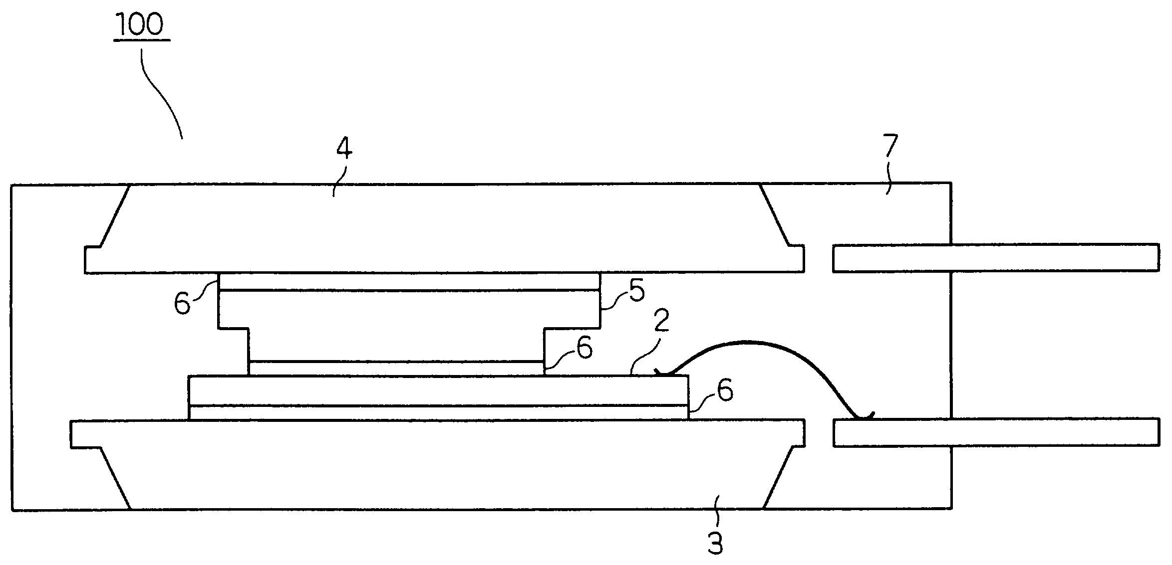
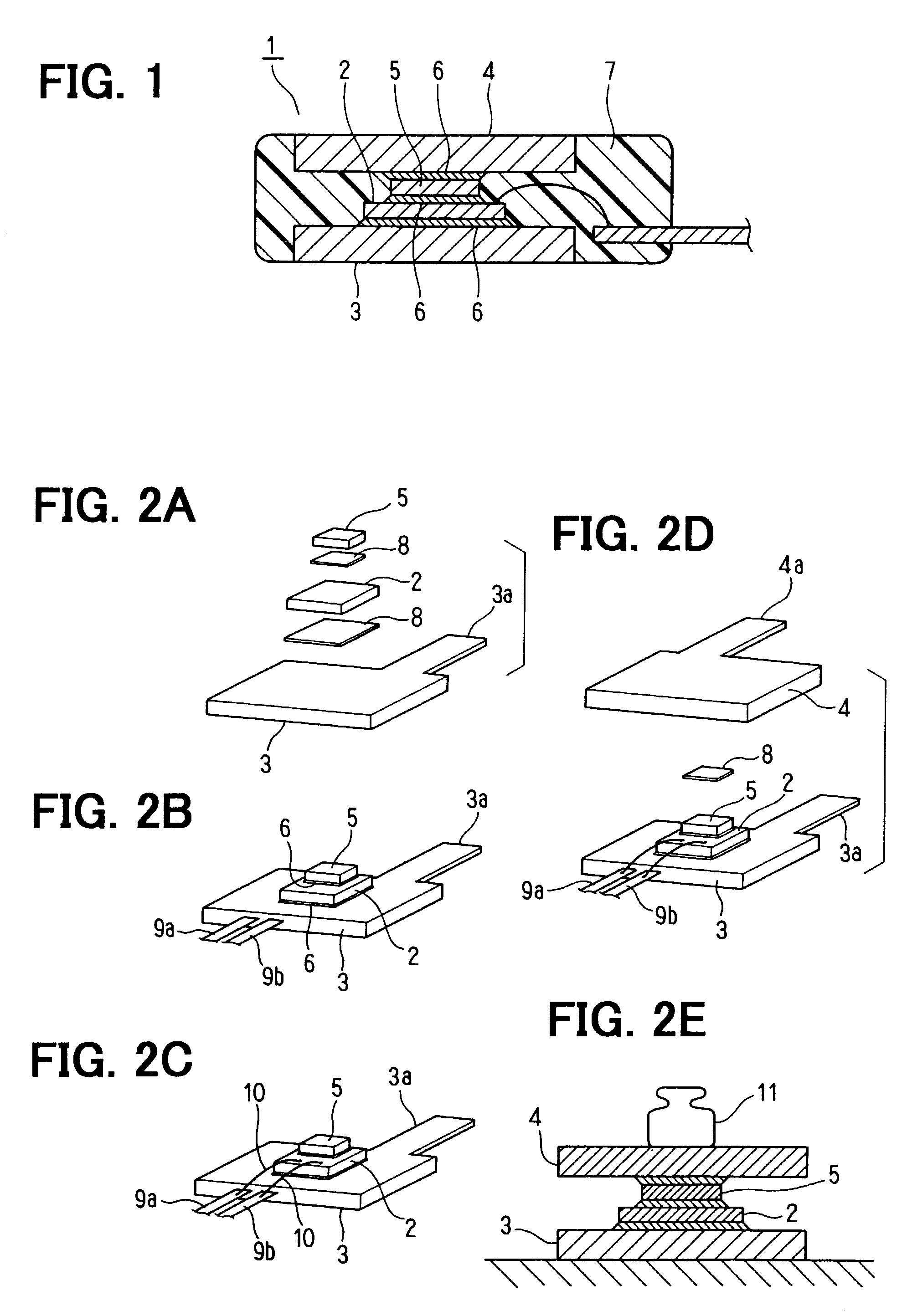
[0054]As shown in FIG. 1, a semiconductor device 1 according to the first embodiment has a similar configuration to the proposed semiconductor device 1A in FIG. 29. The semiconductor device 1 includes a semiconductor chip 2, a lower heat sink 3 (first metal plate), an upper heat sink 4 (second metal plate), and a bridging chip 5 (third metal plate). As viewed in FIG. 1, a lower surface (first surface) of the semiconductor chip 2 and an upper surface of the lower heat sink 3 are joined by a solder 6 (bonding layer). Furthermore, an upper surface (second surface) of the semiconductor chip 2 and a lower surface of the bridging chip 5 are also joined by another solder 6. An upper surface of the bridging chip 5 and a lower surface of the upper heat sink 4 are also joined by other solder 6. The semiconductor chip 2 in FIG. 1 releases heat from both sides of the semiconductor chip 2 through the heat sinks 3, 4.

[0055]The semiconductor chip 2 in FIG. 1 is a vertical power MOS transistor...

second embodiment

[0075

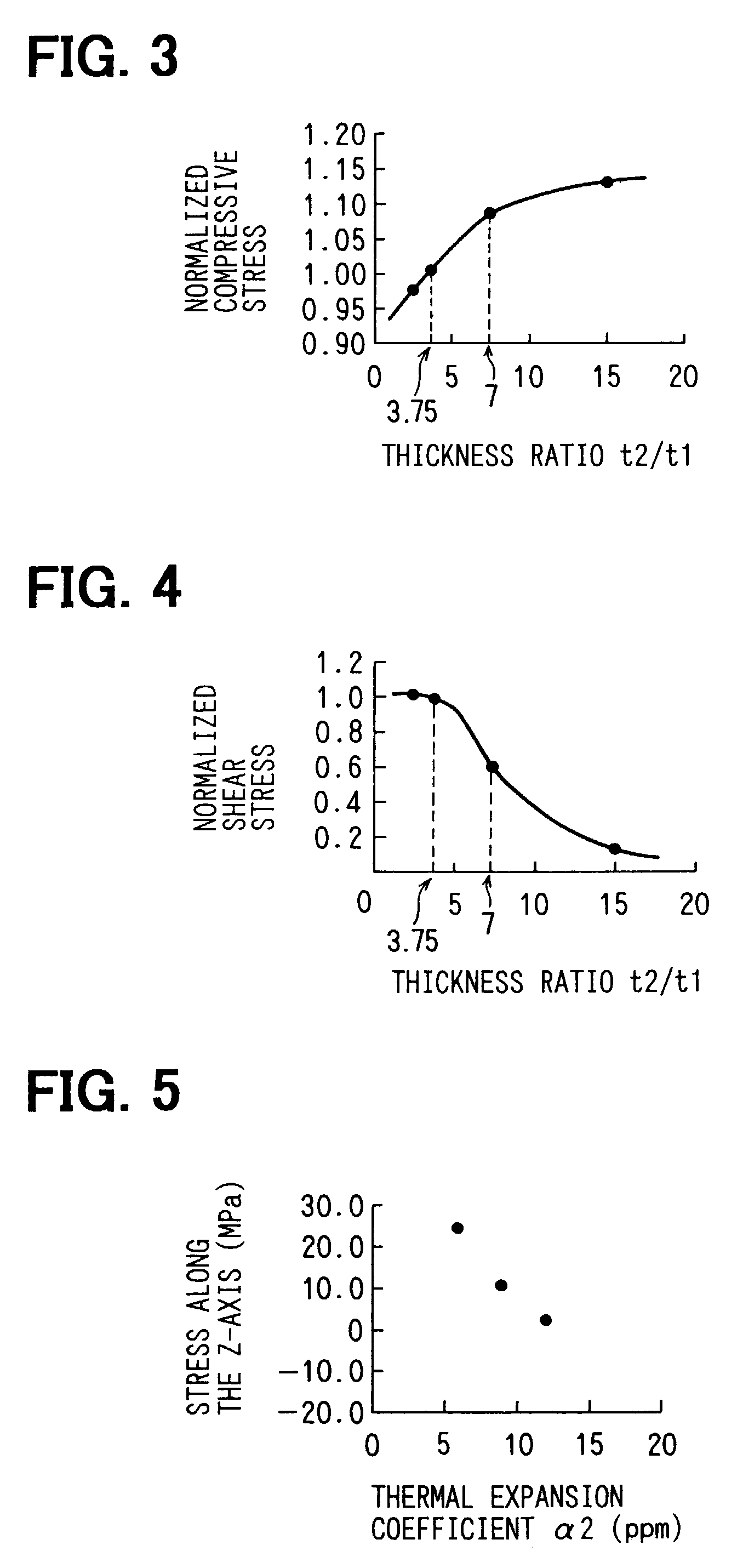
[0076]In the semiconductor device 1, which is shown in FIG. 1, according to the second embodiment, the thermal expansion coefficient α1 of the heat sinks 3, 4 and the thermal expansion coefficient α2 of the resin 7 are set to satisfy the following equation.

0.5≦α2 / α1≦1.5

[0077]By setting the thermal expansion coefficients α1 and α2 this way, it is possible to balance the tensile stress in the semiconductor chip 2 and the shear stress at the surface of the semiconductor chip 2, as described below.

[0078]As shown in FIGS. 5 and 33, the tensile stress in the semiconductor chip 2 at an end of the chip 2 decreases as the coefficient α2 of the resin 7 is increased. The tensile stress is the stress along the Z-axis, which is in the vertical direction of FIG. 1, and has been calculated by simulation for various semiconductor devices 1 having a different thermal expansion coefficient α2 for the resin 7. In the graph in FIGS. 5 and 33, the X-axis represents the thermal expansion coefficient...

third embodiment

[0085

[0086]In the semiconductor device 1 in FIG. 1, according to the third embodiment of the present invention, the surface roughness Ra of the lower surface of the semiconductor chip 2, which faces the lower heat sink 3 satisfies the following equation.

Ra≦500 nm

[0087]As shown in FIG. 8, if the roughness Ra is equal to 500 nm or smaller, it is possible to prevent the semiconductor chip 2 from cracking under a relatively large thermal stress. FIG. 8 shows the percentage of the semiconductor chip 2 that broke when various prototypes of the semiconductor device 1, which have a different surface roughness Ra, are exposed to the thermal stress.

[0088]In the semiconductor device 1 in FIG. 1, the roughness Ra of the lower surface of the semiconductor chip 2 satisfies an equation of Ra≦500 nm, while the condition for the thickness ratio t2 / t1 according to the first embodiment and the condition for the thermal expansion coefficients α1, α2 according to the second embodiment are satisfied. How...


PUM

PropertyMeasurementUnit
tensile stressaaaaaaaaaa
compressive stressaaaaaaaaaa
internal stressaaaaaaaaaa

Abstract

A semiconductor device includes a semiconductor chip that generates heat in operation, a pair of heat sinks for cooling the chip, and a mold resin, in which the chip and the heat sinks are embedded. The thickness t1 of the chip and the thickness t2 of one of heat sinks that is joined to the chip using a solder satisfy the equation of t2/t1≧5. Furthermore, the thermal expansion coefficient α1 of the heat sinks and the thermal expansion coefficient α2 of the mold resin satisfy the equation of 0.5≦α2/α1≦1.5. In addition, the surface of the chip that faces the solder has a roughness Ra that satisfies the equation of Ra≦500 nm. Moreover, the solder is a Sn-based solder to suppress relaxation of a compressive stress in the chip, which is caused by the creeping of the solder.

Description

CROSS REFERENCE TO RELATED APPLICATION[0001]This application is based on and incorporates herein by reference Japanese Patent Applications No. 2002-196140 filed on Jul. 4, 2002, No. 2001-225963 filed on Jul. 26, 2001, and No. 2002-86408 filed on Mar. 26, 2001.BACKGROUND OF THE INVENTION[0002]The present invention relates to a transfer molded power device, which includes a semiconductor chip that generates heat in operation and a heat sink for cooling the semiconductor chip.[0003]A power device, which includes a semiconductor chip and only one heat sink, which is a copper plate for heat release and also functions as an electrode, is proposed. In the power device, power and ground lines are provided as bonding wires. However, this type of power device has the following problems when the semiconductor chip is downsized for reducing the manufacturing costs. For the downsizing, it becomes necessary to reduce the number of bonding wires, so it becomes impossible to supply a predetermined ...

Claims


Application Information

Patent Timeline
Patent Type & Authority Patents(United States)
IPC IPC(8): H01L23/10H01L23/28H01L21/301H01L23/36H01L21/56H01L23/367H01L23/373H01L23/433
CPCH01L21/565H01L23/367H01L23/3736H01L23/4334H01L24/32H01L24/33H01L24/73H01L24/83H01L2224/29111H01L2224/32014H01L2224/32245H01L2224/48091H01L2224/48247H01L2224/48472H01L2224/73215H01L2224/73265H01L2924/01013H01L2924/01029H01L2924/01033H01L2924/01039H01L2924/01047H01L2924/0105H01L2924/01051H01L2924/01078H01L2924/01079H01L2924/01082H01L2924/01088H01L2924/10158H01L2924/13055H01L2924/13091H01L2924/18301H01L2924/30107H01L2924/0132H01L24/48H01L2924/01006H01L2924/01068H01L2924/15724H01L2924/15747H01L2224/92247H01L2924/10253H01L2224/83101H01L2224/83203H01L2224/83815H01L2224/33181H01L2924/1301H01L2924/1305H01L2924/00014H01L2924/00H01L2924/3512H01L2924/351H01L2924/181H01L2224/05624H01L2224/33H01L24/45H01L2224/45124H01L2224/45144H01L2224/85399H01L2224/2612H01L2924/00012H01L2224/45015H01L2924/207H01L23/36
Inventor HIRANO, NAOHIKOTESHIMA, TAKANORINAKASE, YOSHIMIYAGI, KENJIOOKURA, YASUSHIMAMITSU, KUNIAKINOMURA, KAZUHITOFUKUDA, YUTAKA
Owner DENSO CORP
Why Eureka
Try Eureka