Optical wiring board, optical bus system, and method of manufacturing optical wiring board

a technology of optical wiring and optical bus system, which is applied in the direction of optics, optical waveguide light guides, instruments, etc., can solve the problems of reducing the increasing the cost of cutting process, and achieves the effect of high degree of freedom in arrangement of optical components and easy manufacturing

Inactive Publication Date: 2006-12-05
FUJIFILM BUSINESS INNOVATION CORP
View PDF12 Cites 7 Cited by
  • Summary
  • Abstract
  • Description
  • Claims
  • Application Information

AI Technical Summary

Benefits of technology

[0009]It is an object of the invention to provide an optical wiring board and an optical bus system which can be easily manufactured and have a high degree of freedom in the arrangement of optical components, and a method of manufacturing such an optical wiring board.

Problems solved by technology

In the optical wiring board disclosed in JP-A-2000-329962, the optical waveguide and the optical fibers are accommodated and positioned in the grooves formed by a cutting process, thereby causing problems in that the cost of the cutting process is increased, and that the degree of freedom in arrangement is lowered.

Method used


Image

  • Optical wiring board, optical bus system, and method of manufacturing optical wiring board
  • Optical wiring board, optical bus system, and method of manufacturing optical wiring board
  • Optical wiring board, optical bus system, and method of manufacturing optical wiring board

Examples


first embodiment

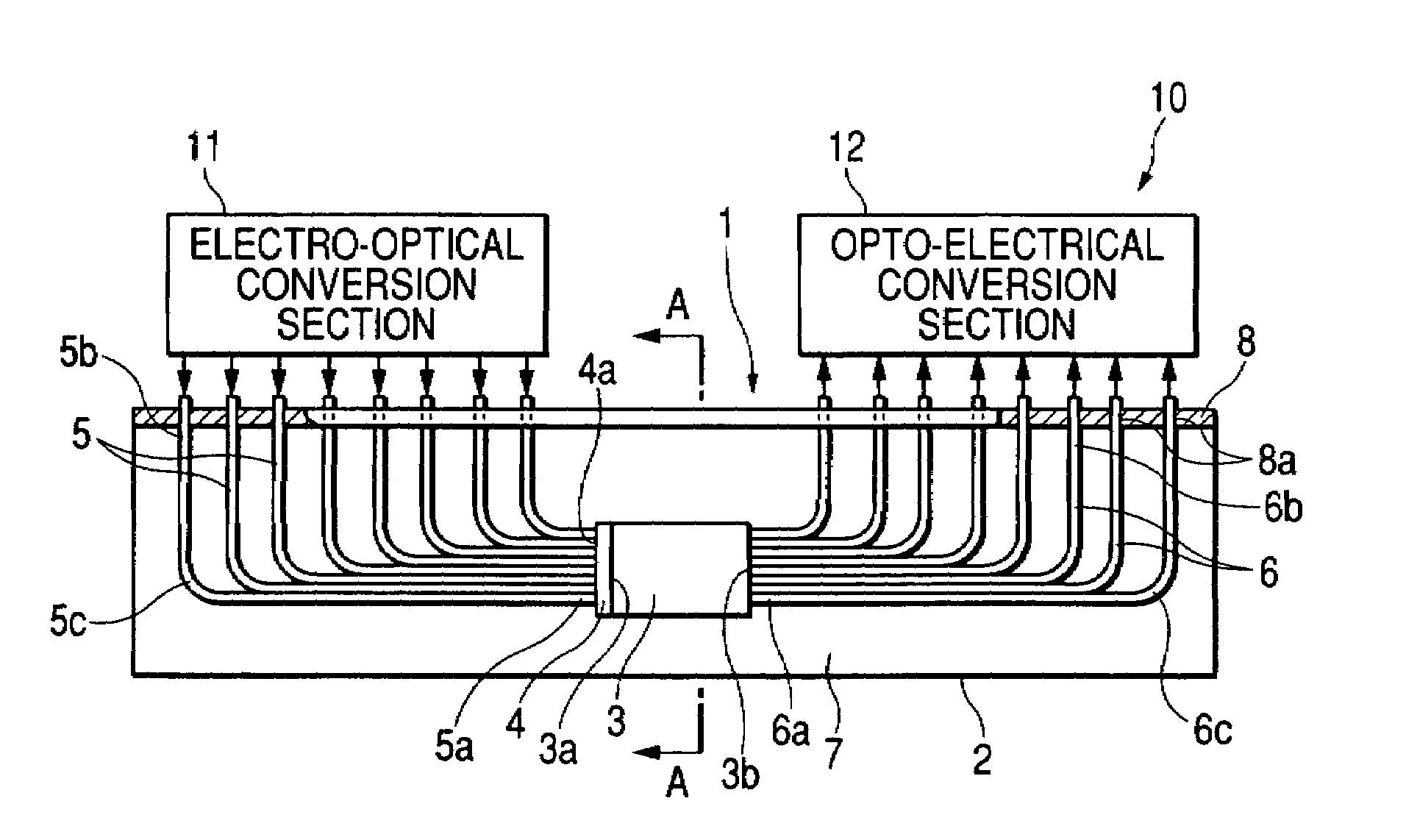
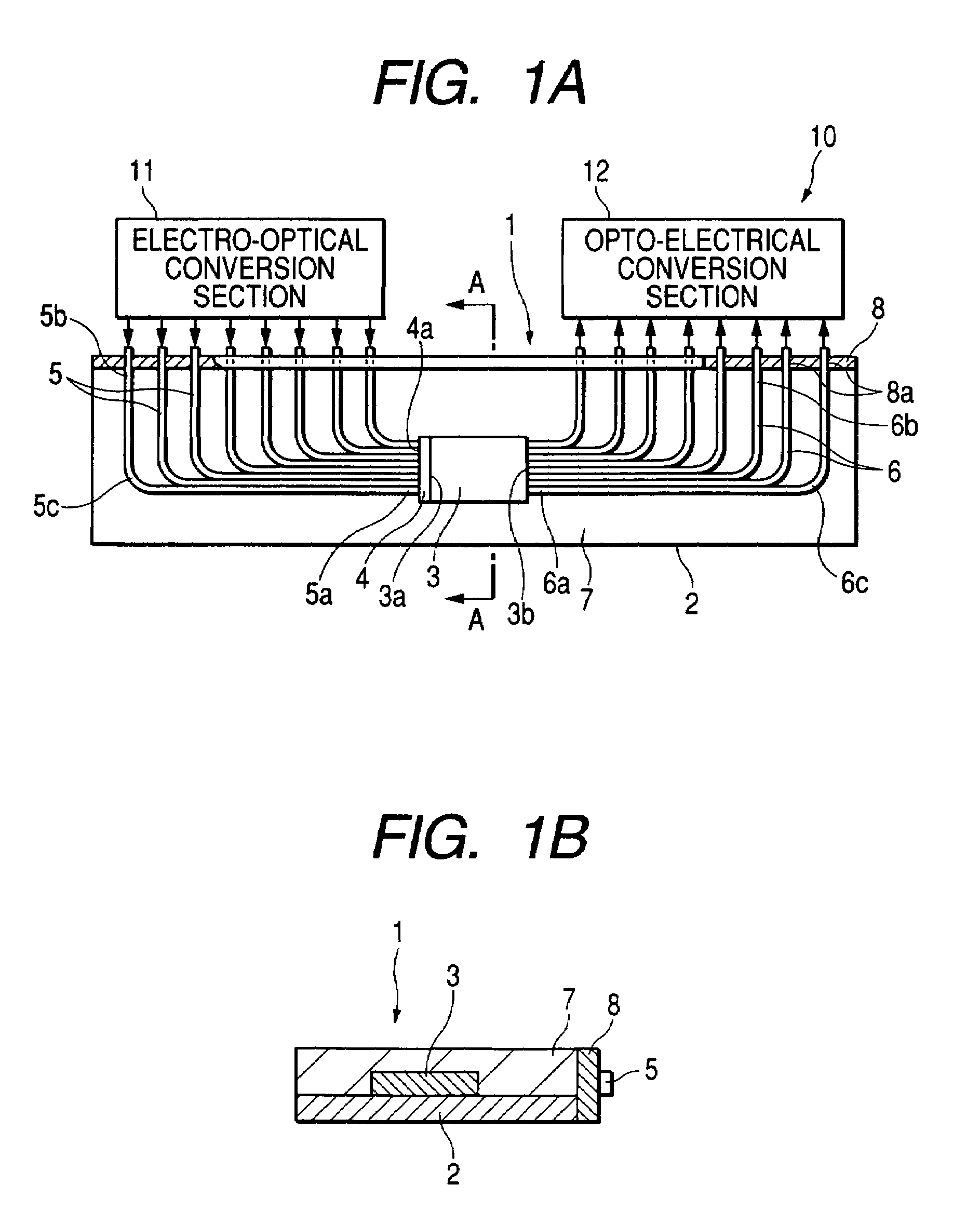
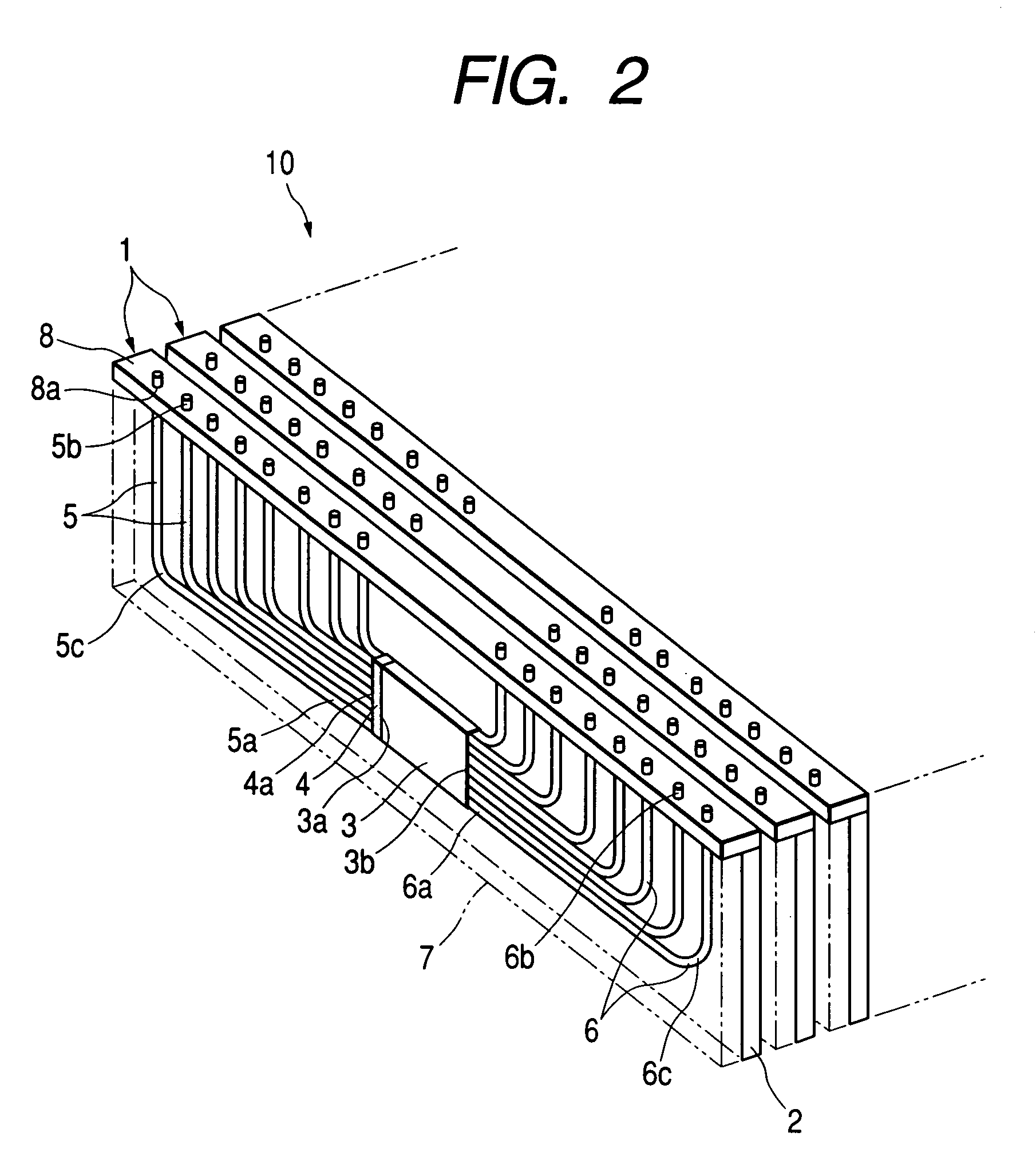
[0023]FIGS. 1 and 2 show an optical bus system of a first embodiment to which an optical wiring board of the invention is applied. FIG. 1A is a plan view, FIG. 1B is a section view taken along the line A—A in FIG. 1A, and FIG. 2 is a perspective view. As shown in FIGS. 1 and 2, the optical bus system 10 includes a plurality of optical wiring boards 1 arranged with forming given gaps therebetween; a plurality of electro-optical conversion circuits 11 which, as shown in FIG. 1A, convert an electric signal into a light signal and supply the light signal to the respective optical wiring boards 1; and a plurality of opto-electrical conversion circuits 12 which convert a light signal output from the respective optical wiring boards 1 into an electric signal.

[0024]Each of the electro-optical conversion circuits 11 and the opto-electrical conversion circuits 12 has a CPU, a memory, and a photoelectric conversion element and is connected to the corresponding optical wiring board 1 via the ph...

third embodiment

[0044]FIGS. 7A to 7D show steps of manufacturing an optical wiring board of the invention. As shown in FIG. 7A, the optical components including the waveguide 3, the transmissive diffusion plate 4, and the first and second optical fibers 5 and 6 are temporarily secured onto the support board 2 by the temporarily securing member as described above. A high viscosity resin 57 is applied so that the resin 7a does not flow between the light incident face 4a of the transmissive diffusion plate 4 and the first optical fibers 5, and then the high viscosity resin 57 is cured as shown in FIG. 7B. The resin 57 has a desired viscosity so long as the resin 57 keeps an applied shape thereof for several tens minutes after applying the resin 57. Preferably, the resin 57 has 5,000 cps or higher in viscosity. More preferably, the resin 57 further has thixotropic characteristic. If the resin 57 has high viscosity and thixotropic characteristic as described above, shape stability thereof after applying...

fourth embodiment

[0047]FIG. 8 shows an optical wiring board of the invention. The optical wiring board 1 includes a support board 2; a planar optical waveguide 3 placed on the support board 2; a plurality of (for example, eight) optical fibers 26 optically connected to one end face 3c of the waveguide 3; a reflective diffusion plate 14 placed on the other end face 3d of the waveguide 3; and a positioning member 8 in which rear ends 26b of the optical fibers 26 are passed through positioning holes 8a to position the rear ends 26b. The optical components including the waveguide 3, the reflective diffusion plate 14, and the optical fibers 26 are sealed by the sealing member 7 made of a resin. Alternatively, the reflective diffusion plate 14 may not be used, and only reflected light may be used. In FIGS. 8, and 9 and 10 which will be described later, the sealing member 7 is shown as a transparent member.

[0048]In the fourth embodiment, an electro-optical circuit section which can convert an electric sign...


PUM


Abstract

In an optical wiring board, an optical components including a planar optical waveguide, a plurality of first optical fibers optically connected via a transmissive diffusion plate to a light incident face of the waveguide, and a plurality of second optical fibers optically connected to a light emitting face of the waveguide is placed on a support board. The optical component is sealed by a sealing member made of a resin.

Description

[0001]The present disclosure relates to the subject matter contained in Japanese Patent Application No.2001-307500 filed on Oct. 3, 2001, which is incorporated herein by reference in its entirety.BACKGROUND OF THE INVENTION[0002]1. Field of the Invention[0003]The present invention relates to an optical wiring board and an optical bus system through which transmission between boards or chips is conducted by means of a light signal, and a method of manufacturing such an optical wiring board, and more particularly relates to an optical wiring board and an optical bus system, which can be manufactured easily and have a high degree of freedom in arrangement of optical components, and a method of manufacturing such an optical wiring board.[0004]2. Description of the Related Art[0005]Conventionally, an optical wiring board in which data are optically transmitted has been proposed for a purpose of increasing the data transmission speed between boards or chips and reducing electromagnetic no...

Claims


Application Information

Patent Timeline
Patent Type & Authority Patents(United States)
IPC IPC(8): G02B6/12G02B6/26G02B6/00G02B6/28G02B6/36
CPCG02B6/3612G02B6/30G02B6/3628G02B6/3676
Inventor NIITSU, TAKEHIROFUNADA, MASAOKOBAYASHI, KENICHIYAMADA, HIDENORIKAMIMURA, TAKESHIOKADA, JUNJIKYOZUKA, SHINYASAKAI, KAZUHIROBABA, TOMOHAMADA, TSUTOMUHISADA, MASASHIOZEKI, SHINOBUTAKANASHI, OSAMUMIURA, MASAAKI
Owner FUJIFILM BUSINESS INNOVATION CORP
Why Eureka
Try Eureka