

Nitride semiconductor light emitting diode and fabrication method thereof
a technology of light-emitting diodes and nitride semiconductors, which is applied in the direction of semiconductor devices, basic electric elements, electrical appliances, etc., can solve the problem of rare high-reflectivity expected, and achieve the effect of improving electrostatic discharge characteristics and minimizing light loss
Active Publication Date: 2006-12-12
SAMSUNG ELECTRONICS CO LTD
View PDF20 Cites 42 Cited by
- Summary
- Abstract
- Description
- Claims
- Application Information
AI Technical Summary
Benefits of technology
The dielectric mirror layer effectively reflects downward-directed light rays, maximizing luminous efficiency and providing excellent ESD characteristics by ensuring high reflectivity and insulation, thereby improving the overall performance of the nitride semiconductor LED.
Problems solved by technology
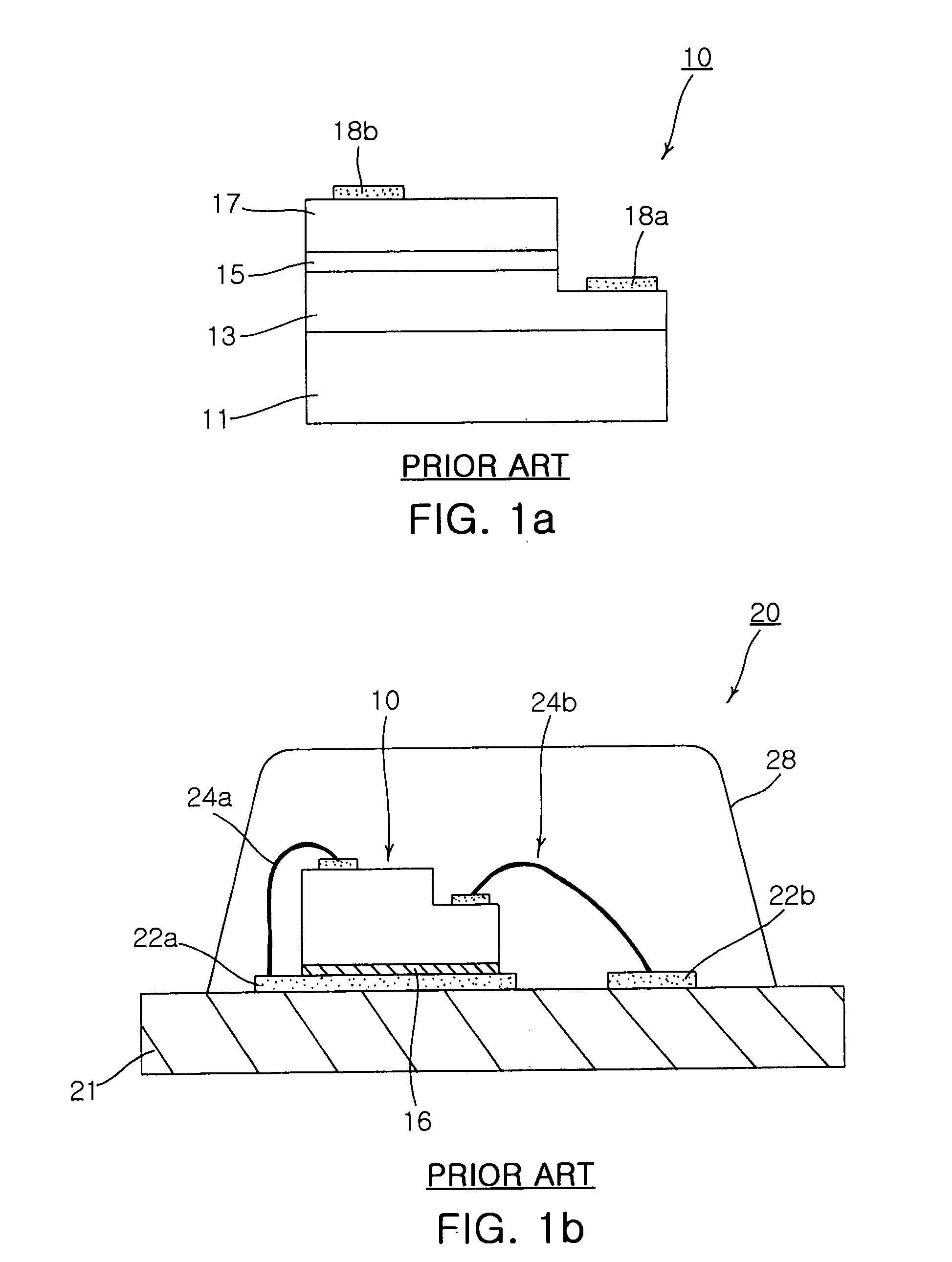
However, because the conductive paste layer 16 itself does not define an irregular surface, high reflectivity can be rarely expected from the conductive paste layer 16 even though it is made of a high reflectivity material such as Ag.
Method used
View moreImage
Smart ImageViewing Examples

Examples
example
[0051]To demonstrate the improvement of brightness in the present invention, GaN LED according to the present invention was produced.
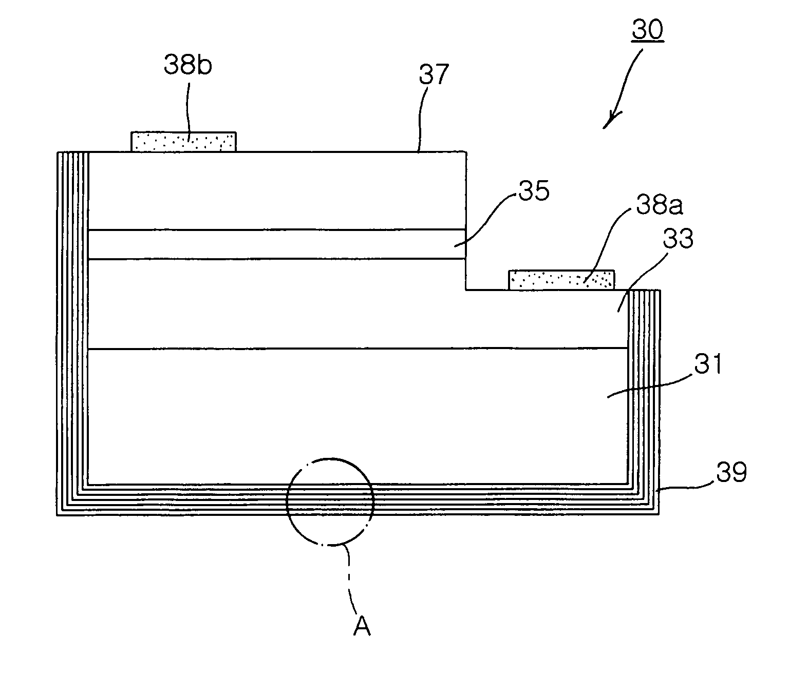
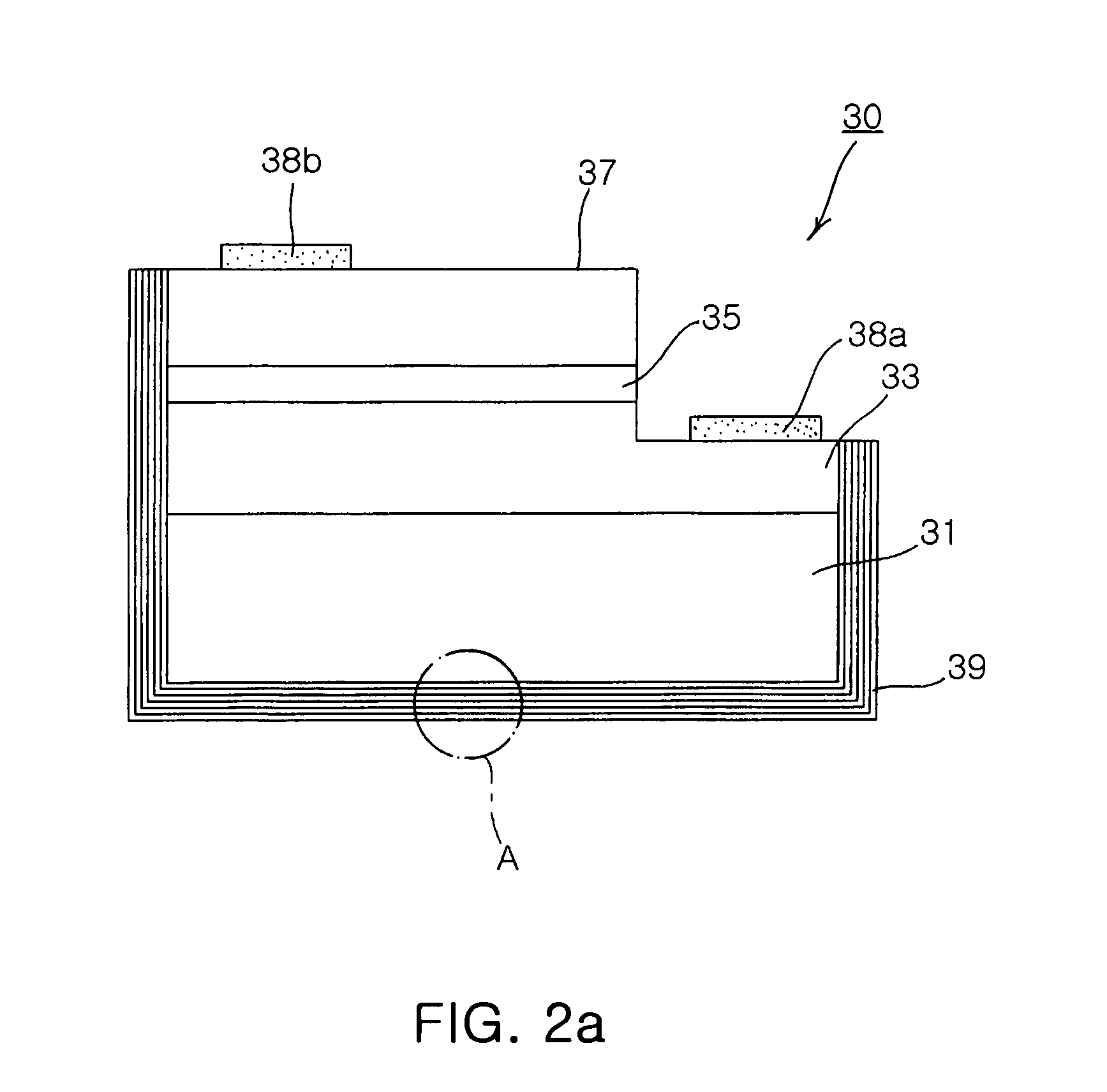
[0052]First, n-type GaN layer, InGaN / GaN MQW active layer and p-type GaN layer were grown on a sapphire substrate sequentially. Then, 7 pairs of Al2O3 film and Si3N4 film were formed as the present dielectric mirror layer on bottom and side surfaces of the resulting structure as the LED shown in FIG. 2A. In this example, the thickness of Al2O3 film was about 700 Å and the thickness of Si3N4 film was about 540 Å.
Login to View More PUM
 Abstract
The invention relates to a nitride semiconductor LED and a fabrication method thereof. In the LED, a first nitride semiconductor layer, an active region a second nitride semiconductor layer of a light emitting structure are formed in their order on a transparent substrate. A dielectric mirror layer is formed on the underside of the substrate, and has at least a pair of alternating first dielectric film of a first refractivity and a second dielectric film of a second refractivity larger than the first refractivity. A lateral insulation layer is formed on the side of the substrate and the light emitting structure. The LED of the invention effectively collimate undesirably-directed light rays, which may be otherwise extinguished, to maximize luminous efficiency, and are protected by the dielectric mirror layer formed on the side thereof to remarkably improve ESD characteristics.
Description
RELATED APPLICATIONS[0001]The present application is based on, and claims priority from, Korean Application Serial Number 2003-95172, filed Dec. 23, 2003, the disclosure of which is hereby incorporated by reference herein in its entirety.BACKGROUND OF THE INVENTION[0002]1. Field of the Invention[0003]The present invention relates to a nitride semiconductor light emitting diode, and more particularly, to a nitride semiconductor light emitting diode and a fabrication method thereof, in which a high reflectivity layer is formed to minimize light loss as well as achieve excellent electrostatic discharge characteristics.[0004]2. Description of the Related Art[0005]As well-known in the art, Nitride semiconductor Light Emitting Diodes (LEDs) are being spotlighted as high power optical devices capable of generating single wavelength light such as blue or green light to realize full color display. A nitride semiconductor LED is made by growing single crystal semiconductor expressed as a form...
Claims
Login to View More Application Information
Patent Timeline
 Patent Type & AuthorityPatents(United States)
IPC IPC(8): H01L27/15H01L29/06H01L29/26H01L31/12H01L33/00H01L33/06H01L33/10H01L33/32H01L33/46H01L33/62
CPCH01L33/46Y10S257/918H01L2224/48091H01L2224/73265H01L2224/49107H01L2924/00014
InventorSEO, JUN HOJANG, JONG HO
OwnerSAMSUNG ELECTRONICS CO LTD