Antenna device and communications apparatus comprising same

a technology of antenna device and communications apparatus, which is applied in the direction of resonant antenna, helical antenna, non-resonant long antenna, etc., can solve the problems of not meeting the demand of thinning, the antenna device of jp 11-4117 a is not suitable for sufficient miniaturization, and the mobile phone is sometimes disconnected, etc., to avoid the effect of gain decrease, wide bandwidth and high average gain

Active Publication Date: 2006-12-12
HITACHI METALS LTD
View PDF16 Cites 81 Cited by
  • Summary
  • Abstract
  • Description
  • Claims
  • Application Information

AI Technical Summary

Benefits of technology

[0012]Accordingly, an object of the present invention is to provide a small antenna device capable of being adapted to multi-band systems, which avoids gain decrease by securing isolation in pluralities of frequency bands, and which has a wide bandwidth and a high average gain in each frequency band.

Problems solved by technology

According to recent rapid expansion of mobile phones, however, a frequency band allocated to each system cannot allow all users to use their mobile phones in major cities in advanced countries, resulting in difficulty in connection and thus causing such a problem that mobile phones are sometimes disconnected during communication.
However, the antenna device of JP 11-4117 A is not suitable for sufficient miniaturization because it comprises two chip antennas in a shape of rectangular parallelepiped.
Though it has been proposed to mount a chip antenna 93b on a rear surface 92b of the substrate 91 for miniaturization, it does not meet the demand of thinning, because the thickness of a mounting substrate hinders such demand.
Thus, the antenna device of JP 11-4117 A fails to satisfy the demands of miniaturization, space reduction and bandwidth increase.
However, the conventional antenna devices are disadvantageous in failing to meet all of the requirements of miniaturization, space reduction and bandwidth increase.
Though U.S. Pat. No. 6,288,680 proposes the bandwidth increase, it simply suppresses the deterioration of bandwidth in a low frequency band, failing to handle a multi-band system.
When pluralities of radiation electrodes are formed in the conventional antenna substrate to make the system adaptable for multi-band, it is difficult to keep isolation because of electrostatic capacitance generated between the radiation electrodes.
Specifically, the higher the electrostatic capacitance between the radiation electrodes, the more the high-frequency current flows in the radiation electrodes in opposite directions, so that the radiation electrodes weaken the radiation of an electromagnetic wave each other, resulting in decrease in the gain (sensitivity).
Though a wide band and a high gain are desirable in pluralities of frequency bands in multi-band antenna devices, JP 11-4117 A and U.S. Pat. No. 6,288,680 fail to provide any discussion on such points.

Method used


Image

  • Antenna device and communications apparatus comprising same
  • Antenna device and communications apparatus comprising same
  • Antenna device and communications apparatus comprising same

Examples


first embodiment

[1]First Embodiment

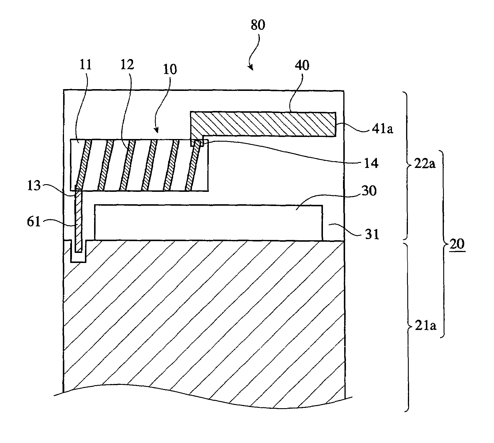
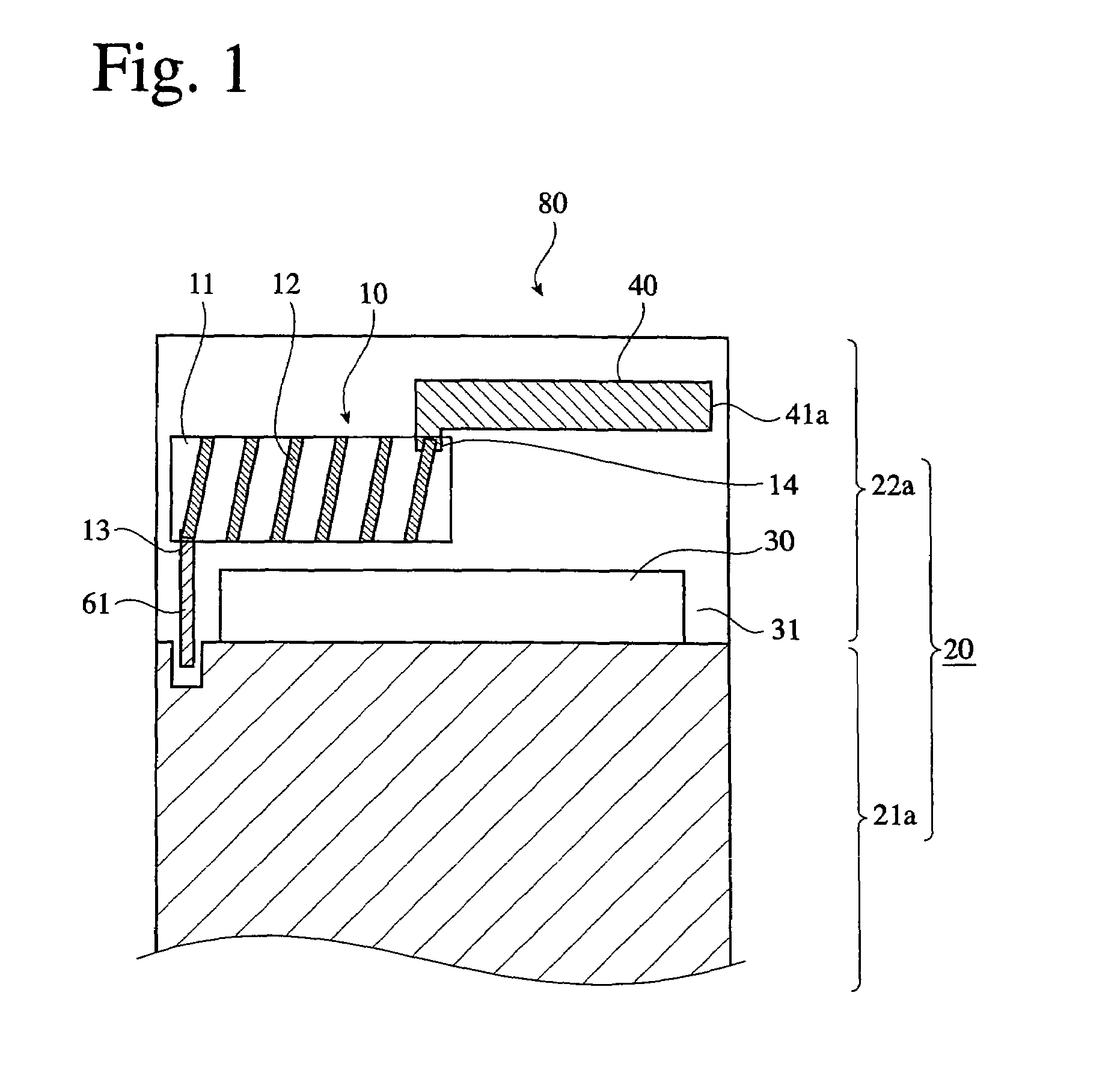
[0079]FIG. 1 shows an antenna device 80 according to one embodiment of the present invention. A mounting substrate 20 comprises a ground portion 21 having a ground electrode pattern, which comprises a ground portion 21a on the chip-antenna-carrying surface, and a ground portion 21b formed on the opposing surface (rear surface) of the chip-antenna-carrying surface, and a non-ground portion 22 having no ground electrode pattern, which comprises a non-ground portion 22a on the chip-antenna-carrying surface, and a non-ground portion 22b on the opposing surface of the chip-antenna-carrying surface. The non-ground portion 22a of the mounting substrate 20 is provided with a chip antenna 10, and a second radiation electrode 40 formed in a linear conductor pattern on the surface carrying the chip antenna 10.

[0080]FIG. 2(a) is a partial plan view of the antenna device when viewed from the side of the surface carrying the chip antenna 10, and FIG. 2(b) is a partial plan view...

second embodiment

[2]Second Embodiment

[0098]FIG. 7 shows an antenna device according to another embodiment of the present invention, which comprises only a chip antenna 10. This antenna device 80 has a bandwidth increased by a hollow groove 30 provided between the chip antenna 10 and a ground portion 21a on a chip-antenna-carrying surface, conducting resonance in as wide a frequency range as 1575–1800 MHz, thereby covering both frequency bands of PCS and GPS. Accordingly, this antenna device 80 is adapted to dual-band. Because the frequency band (1800 MHz) of PCS is relatively close to the frequency band (1575 MHz) of GPS, it is adapted to dual-band with one chip antenna 10. In the present invention, a second radiation electrode is preferably formed, though it may be omitted in some cases, for instance, in an antenna using a single frequency with a narrow bandwidth. Even in such cases, bandwidth increase is obtained by the hollow groove. This is also within the scope of the present invention.

third embodiment

[3]Third Embodiment

[0099]FIG. 8 shows an antenna device, in which a chip antenna 10 is mounted onto one surface of a mounting substrate 20, and a second radiation electrode 40 is formed on the other surface (rear surface) of the mounting substrate 20. In this embodiment, a terminal electrode 14 extends on a surface of the mounting substrate 20, and a first radiation electrode 12 on the chip antenna 10 is connected to the second radiation electrode 40, via a through-hole 19 (depicted by a black circle on the front side and a white circle on the rear side) formed in the mounting substrate 20. This embodiment provides a dual-band antenna device having a cellular band of 800 MHz and a GPS band of 1575 MHz, by interaction between the first radiation electrode 12 and the second radiation electrode 40. On the cellular band side, an open end 41a of the second radiation electrode 40 is distant from a power-supplying electrode 13 to increase the effective electric length, thereby making the a...


PUM


Abstract

An antenna device comprising (a) a mounting substrate having a ground portion and a non-ground portion, (b) a chip antenna mounted onto said non-ground portion, which comprises a substrate, a first radiation electrode formed on said substrate, a power-supplying electrode connected or not connected to the other end of said first radiation electrode, and a terminal electrode connected or not connected to one end of said first radiation electrode, and (c) at least one second radiation electrode formed in a conductor pattern on said non-ground portion, said second radiation electrode having one end connected or not connected to said terminal electrode and the other end which is an open end, and a cavity existing between said chip antenna and / or said second radiation electrode and said ground portion.

Description

FIELD OF THE INVENTION[0001]The present invention relates to an antenna device used in mobile phones, wireless local area networks (LANs), etc., particularly to a small, wide-bandwidth antenna device adaptable to multi-bands such as dual-band and triple-band, and a communications apparatus comprising such an antenna.BACKGROUND OF THE INVENTION[0002]The demand of miniaturization on communications apparatus and electronic apparatuses such as mobile phones and personal computers necessitates the miniaturization of antenna devices used therein. Thus, chip antennas comprising power-supplying electrodes and radiation electrodes on or in base substrates made of dielectric or magnetic materials have become used.[0003]There are various systems for mobile phones, for instance, EGSM (extended global system for mobile communications) and DCS (digital cellular system) widely used mostly in Europe, PCS (personal communications services) used in the U.S., and various systems using TDMA (time divis...

Claims


Application Information

Patent Timeline
Patent Type & Authority Patents(United States)
IPC IPC(8): H01Q1/24H01Q1/36H01Q1/38H01Q9/30H01Q11/08H01Q21/30H01Q23/00
CPCH01Q1/243H01Q1/362H01Q1/38H01Q9/30H01Q11/08H01Q21/30H01Q23/00
Inventor TAKAKI, YASUNORIAOYAMA, HIROYUKI
Owner HITACHI METALS LTD
Why Eureka
Try Eureka