Display device using light-emitting elements

Inactive Publication Date: 2006-12-12
LAPIS SEMICON CO LTD
View PDF12 Cites 8 Cited by
  • Summary
  • Abstract
  • Description
  • Claims
  • Application Information

AI Technical Summary

Benefits of technology

[0008]An object of the present invention is to provide a display device wherein the change of the amount of light of the light-emitting elements caused by change of the number of light-emitting elements that emit light simultaneously is small.
[0010]The control circuit suppresses change of the voltage between the anode and cathode of the light-emitting elements caused by change of the number of light-emitting elements that emit light simultaneously. In this way, change of the amount of light of the light-emitting elements is suppressed.

Problems solved by technology

With such a construction, when a large number of organic EL elements emit light simultaneously, the amount of current flowing to ground becomes very large.

Method used


Image

  • Display device using light-emitting elements
  • Display device using light-emitting elements
  • Display device using light-emitting elements

Examples


first embodiment

[0021

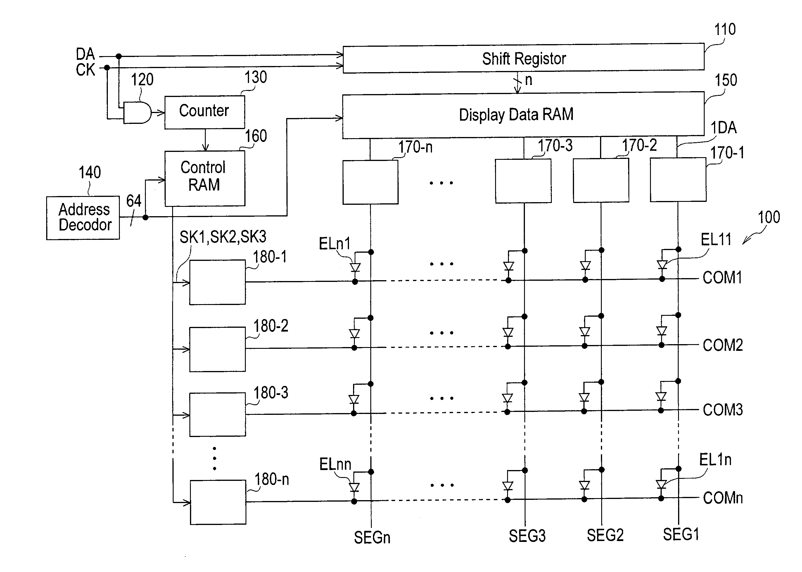
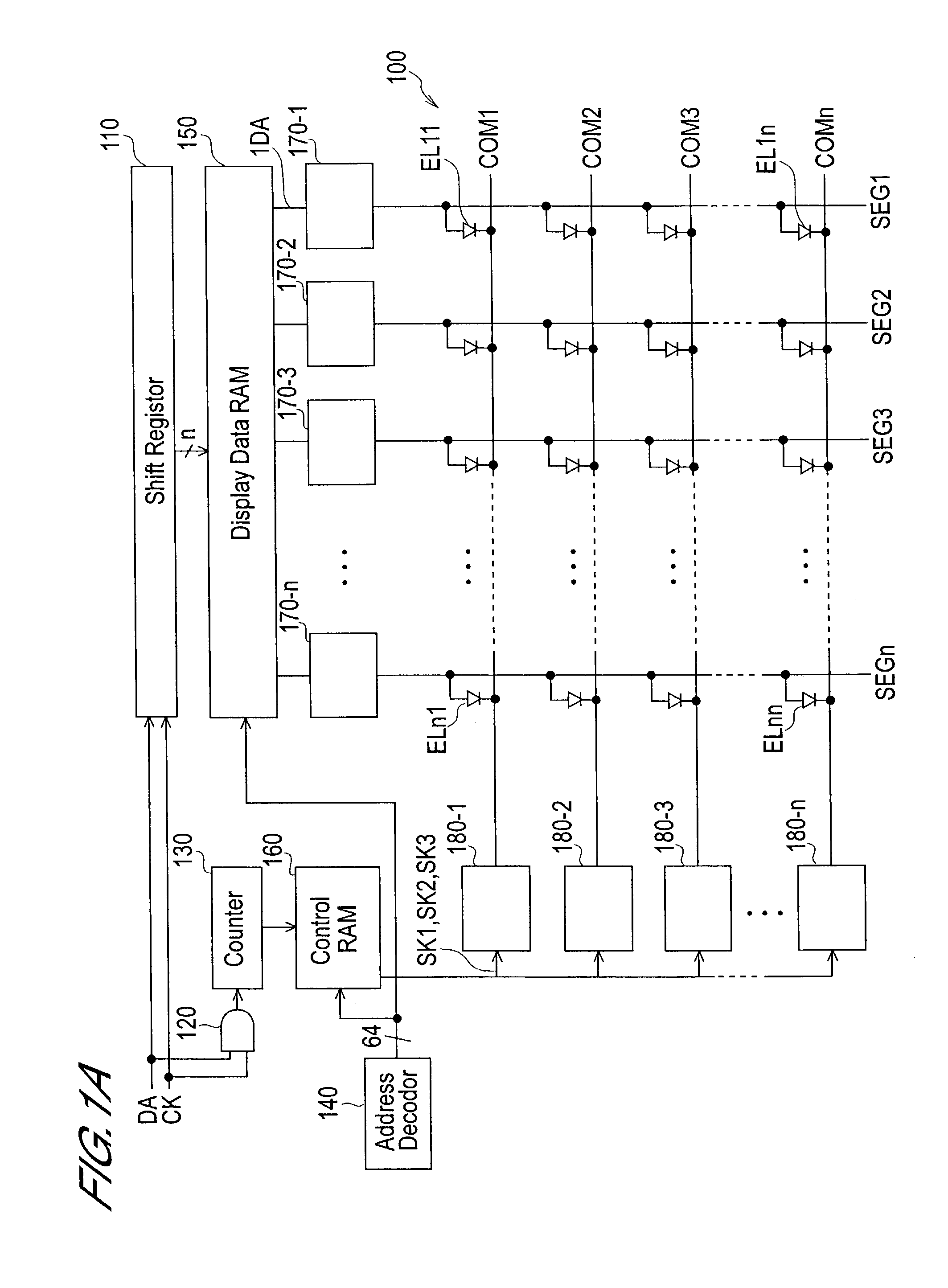
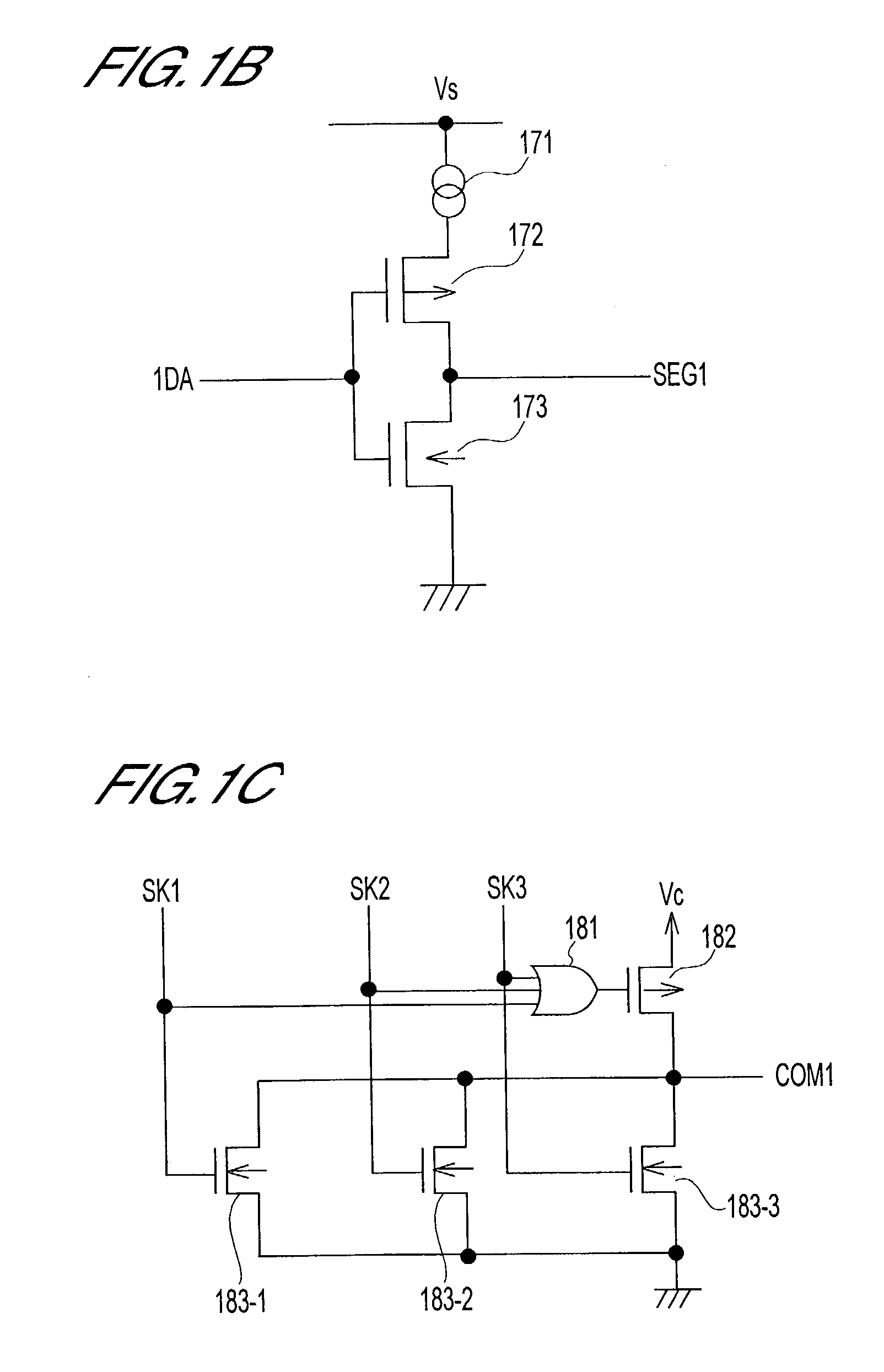
[0022]FIG. 1A to FIG. 1C are circuit diagrams illustrating the layout of a display device according to a first embodiment of the present invention.

[0023]As shown in FIG. 1A, this matrix type display device comprises a display panel 100, a shift register 110, AND gate 120, display number counter 130, address decoder 140, display data RAM (random access memory) 150, negative electrode control RAM 160, positive electrode output circuits 170-1 to 170-n and negative electrode output circuits 180-1 to 180-n.

[0024]Display panel 100 comprises n×n (for example 128×128) organic EL elements EL11 to ELnn, data lines SEG1 to SEGn and scanning lines COM1 to COMn. EL elements of the same column are connected with the same data line. Also, EL elements of the same row are connected with the same scanning line.

[0025]Shift register 110 inputs serial display data DA with a timing supplied by clock CK and converts the data DA into n-bit parallel signals. In the display data of the present embodimen...

second embodiment

[0046

[0047]FIG. 3A and FIG. 3B are circuit diagrams illustrating the layout of a display device according to a second embodiment of the present invention. In FIG. 3A, structural elements given the same reference symbols as in FIG. 1A are respectively the same as in FIG. 1A.

[0048]As shown in FIG. 3A, a display device according to this embodiment comprises a decoder 310. In addition, the internal construction of negative electrode output circuits 320-1 to 320-n of the display device of this embodiment differs from the first embodiment.

[0049]Decoder 310 inputs a negative electrode control signal from negative electrode control RAM 160 and outputs gate control signals. Here, outputs gate control signals G1, G2, . . . , G8 are input to the negative electrode output circuits 320-1. The number of gate control signals and G1 to G8 which are high-level signals is determined in accordance with the value of the binary number indicated by the negative electrode control signal. For example, when...

third embodiment

[0060

[0061]FIGS. 4A and 4B is a circuit diagram illustrating the construction of a display device according to a third embodiment of the present invention. In FIG. 4A structural elements that have the same reference symbols as in FIG. 1A are respectively the same as in FIG. 1A.

[0062]As shown in FIG. 4A and FIG. 4B, a display device according to this embodiment comprises a negative electrode controller 410. Furthermore, the internal structure of the negative electrode output circuits 420-1 to 420-n of the display device of this embodiment is different from that of the first embodiment.

[0063]FIG. 4B is a circuit diagram illustrating the internal structure of negative electrode controller 410 and negative electrode output circuit 420-1. Only portions of the negative electrode controller 410 of FIG. 4B that are associated with negative electrode output circuit 420-1 are illustrated.

[0064]Negative electrode controller 410 comprises an OR gate 411 and a digital / analogue converter 412. OR ...


PUM


Abstract

Display device wherein change of the amount of light of the light-emitting elements caused by change of the number of light-emitting elements that emit light simultaneously is small. This display device includes a display panel having light-emitting elements arranged in matrix fashion; data lines for applying anode potential to light-emitting elements of the same column; scanning lines for applying cathode potential to light-emitting elements of the same row; and a control circuit that adjusts voltage between the anode and cathode of the light-emitting elements based on the number of light-emitting elements that emit light simultaneously. The control circuit suppresses changes of voltage between the anode and cathode of the light-emitting elements caused by a change in the number of light-emitting elements that emit light simultaneously. Accordingly, change of the amount of light of the light-emitting elements is suppressed.

Description

BACKGROUND OF THE INVENTION[0001]1. Field of the Invention[0002]The present invention relates a display device using organic electroluminescence elements, light-emitting diodes or other similarly light-emitting elements. More particularly, the present invention relates to a display device having a driving circuit which can suppresses changes of light emission intensity of the light emitting elements.[0003]2. Description of the Related Art[0004]Display devices are known employing for example organic EL (electroluminescence) elements. Organic EL elements can be driven with low DC voltage. In addition, organic EL elements are light-emitting elements, so, compared with optically transparent elements such as liquid-crystal elements, they provide a wide field of view angle, a bright display surface and are of small thickness and light weight. Organic EL elements can therefore be employed as large-capacity display devices for various applications.[0005]A technique for driving organic EL di...

Claims


Application Information

Patent Timeline
IPC IPC(8): G09G3/30G09G3/32H01L51/50G09G3/20
CPCG09G3/3216G09G3/3266G09G3/3283G09G2320/0233G09G2360/16
Inventor TAMAKI, TAKASHI
Owner LAPIS SEMICON CO LTD
Why Eureka
Try Eureka