Display apparatus for sequential pixel sampling including attenuated capacitive coupling between signal lines

Inactive Publication Date: 2006-12-12
SONY CORP
View PDF3 Cites 3 Cited by
  • Summary
  • Abstract
  • Description
  • Claims
  • Application Information

AI Technical Summary

Benefits of technology

[0019]In order to solve the above problem of the related art, the following means are provided. That is, there is provided a display apparatus including: a pixel array unit having gate lines in a form of rows, signal lines in a form of columns, and pixels arranged in a form of a matrix at intersections of the gate lines and the signal lines; a vertical driving circuit connected to the gate lines, for sequentially selecting rows of the pixels; and a horizontal driving circuit connected to the signal lines, for operating on the basis of a predetermined clock signal and sequentially writing a video signal to pixels of a selected row. The horizontal driving circuit includes: a shift register for performing shift operation in synchronism with the clock signal and sequentially outputting shift pulses from respective shift stages; a shaping switch group for shaping the shift pulses sequentially outputted from the shift register and sequentially outputting non-overlap sampling pulses temporally separated from each other; and a sampling switch group for sequentially sampling the input video signal in a non-overlapping manner in response to the sampling pulses and supplying the sampled video signal to each of the signal lines. A capacitance interposed between adjacent signal lines is connected to wiring of lower impedance than a signal line side, thereby attenuating capacitive coupling between the adjacent signal lines and thus suppressing the potential variation of the video signal sampled in a non-overlapping manner and supplied to the signal lines.
[0021]According to the present invention, in the dot-sequential type active matrix display apparatus, the capacitance interposed between the adjacent signal lines is connected to the wiring of low impedance. With this layout, it is possible to suppress the picture defect in the form of a vertical streak caused by coupling between the adjacent signal lines even when performing non-overlap sampling driving introduced as a measure against the vertical streak and for increasing the ghost margin.

Problems solved by technology

As a result, the variation in the sampled potential appears as a vertical streak on the display screen, thus degrading picture quality.
When the number of pixels in a horizontal direction, in particular, is increased with higher definition in the active matrix liquid crystal display apparatus of the dot-sequential driving type, it is difficult to secure a sufficient sampling time for the sequential sampling for all the pixels of the video signal “video” inputted by one system within a limited horizontal effective period.
As described above, the active matrix display apparatus of the dot-sequential type conventionally has problems of the vertical streak defect and the insufficient ghost margin.
However, a new picture quality defect is caused by the introduction of this non-overlap sampling driving.
This vertical streak defect cannot be completely eliminated even when the potential of each signal line is adjusted in advance by a precharge signal, thus presenting a problem to be solved.

Method used


Image

  • Display apparatus for sequential pixel sampling including attenuated capacitive coupling between signal lines
  • Display apparatus for sequential pixel sampling including attenuated capacitive coupling between signal lines
  • Display apparatus for sequential pixel sampling including attenuated capacitive coupling between signal lines

Examples


Embodiment Construction

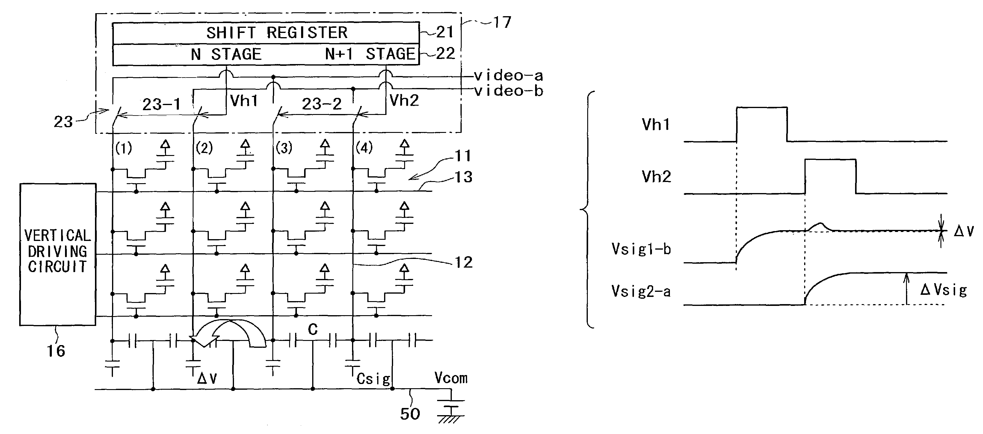
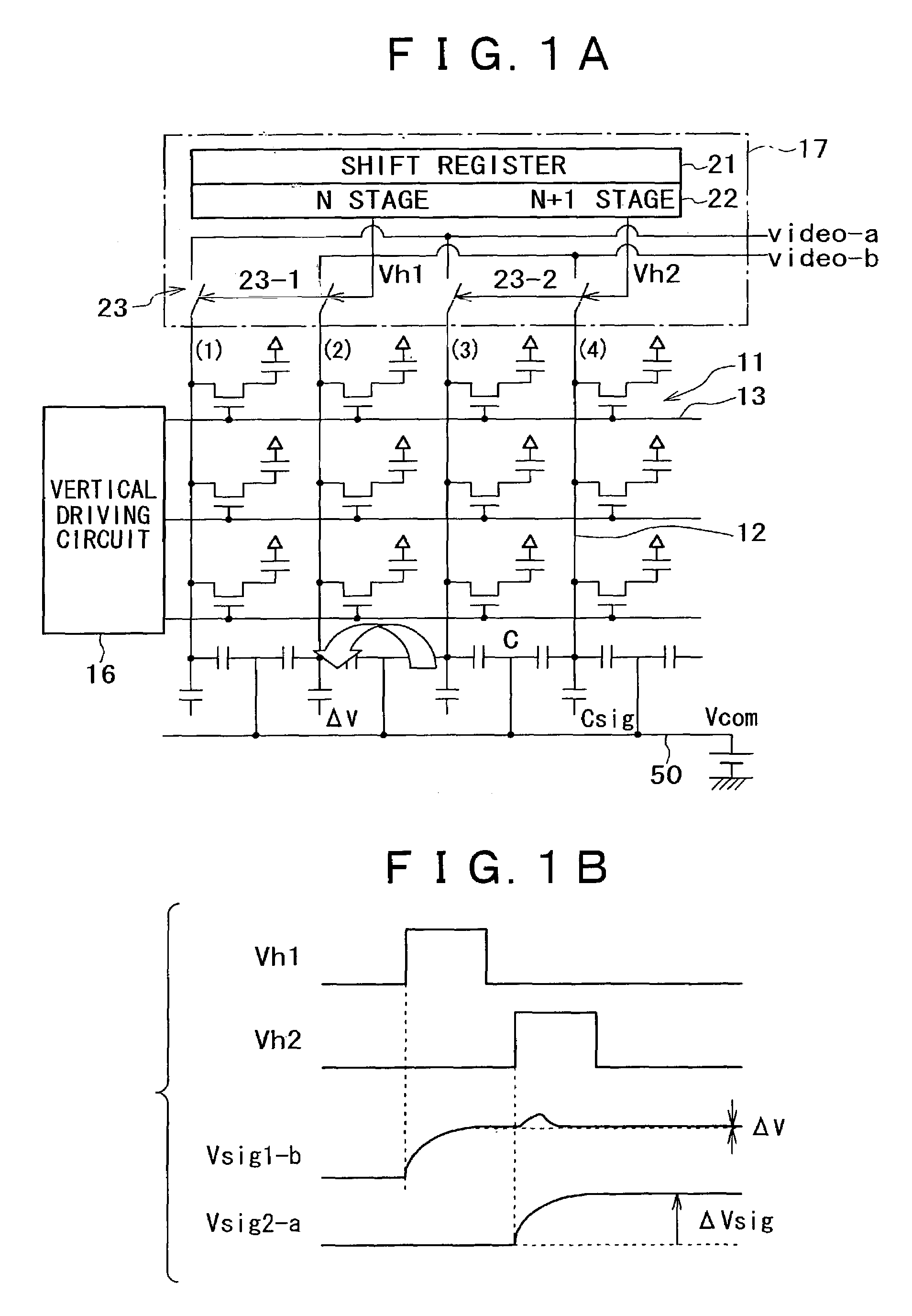
[0036]A preferred embodiment of the present invention will hereinafter be described in detail. FIGS. 1A and 1B are respectively a schematic block diagram showing a basic configuration of a display apparatus according to the present invention and a waveform chart. As shown in FIG. 1A, the display apparatus includes a pixel array unit, a vertical driving circuit 16, and a horizontal driving circuit 17. The pixel array unit includes gate lines 13 in a form of rows, signal lines 12 in a form of columns, and pixels 11 arranged in a form of a matrix at intersections of the gate lines 13 and the signal lines 12. In the present embodiment, a pixel 11 includes a switching element formed by a thin film transistor and a liquid crystal cell. The thin film transistor has a gate electrode connected to a corresponding gate line 13, a source electrode connected to a corresponding signal line 12, and a drain electrode connected to a corresponding liquid crystal cell. The liquid crystal cell includes...


PUM


Abstract

The present invention provides a display apparatus including a pixel array unit, a vertical driving circuit, and a horizontal driving circuit. The horizontal driving circuit includes a shift register for performing shift operation in synchronism with the clock signal and sequentially outputting shift pulses from respective shift stages, a shaping switch group for shaping the shift pulses sequentially outputted from the shift register and sequentially outputting non-overlap sampling pulses temporally separated from each other, and a sampling switch group for sequentially sampling the input video signal in a non-overlapping manner in response to the sampling pulses and supplying the sampled video signal to each of the signal lines. A capacitance interposed between adjacent signal lines is connected to wiring of lower impedance than a signal line side, thereby attenuating capacitive coupling between the adjacent signal lines and thus suppressing the potential variation of the video signal sampled in a non-overlapping manner and supplied to the signal lines.

Description

[0001]This application claims priority to Japanese Patent Application Number JP 2002-145620 filed May 21, 2002 which is incorporated herein by reference.BACKGROUND OF THE INVENTION[0002]The present invention relates to a display apparatus, and particularly to a dot-sequential driving active matrix display apparatus using a so-called non-overlap sampling method for a horizontal driving circuit thereof.[0003]In a display apparatus, for example an active matrix liquid crystal display apparatus using a liquid crystal cell as a display element (electro-optical element) of a pixel, a horizontal driving circuit of a dot-sequential driving type using a clock driving method, for example, is known. FIG. 8 shows a conventional example of the clock driving type horizontal driving circuit. In FIG. 8, the horizontal driving circuit 100 has a shift register 101, a clock extracting switch group 102, and a sampling switch group 103.[0004]The shift register 101 includes n shift stages (transfer stage...

Claims


Application Information

Patent Timeline
IPC IPC(8): G09G3/36G02F1/1345G02F1/133G09G3/20
CPCG09G3/3688G09G2320/0209G09G2310/0297G09G2310/0248G09G3/36
Inventor YAMASHITA, JUNICHIUCHINO, KATSUHIDE
Owner SONY CORP
Why Eureka
Try Eureka