
Liquid crystal device and electronic equipment

a technology of liquid crystal and electronic equipment, applied in the direction of refrigerating machines, instruments, corrosion prevention, etc., can solve the problems of increasing costs, and achieve the effect of low cost and less roughness

Active Publication Date: 2006-12-12
138 EAST LCD ADVANCEMENTS LTD
View PDF27 Cites 0 Cited by
  • Summary
  • Abstract
  • Description
  • Claims
  • Application Information

AI Technical Summary

Benefits of technology

This approach reduces image roughness and enhances display quality with high contrast and wide-angle visibility at a lower cost by stabilizing liquid crystal alignment and eliminating the need for complex electrode patterning, while maintaining high-quality image display in low-voltage applications.

Problems solved by technology

However, in the structure described above, a new process of patterning of the common electrode is required for the opposed substrate in addition to a pattern forming process for the light shielding film and a common electrode forming process, which results in the cost increase.

Method used


Image

  • Liquid crystal device and electronic equipment
  • Liquid crystal device and electronic equipment
  • Liquid crystal device and electronic equipment

Examples


first exemplary embodiment

[0028

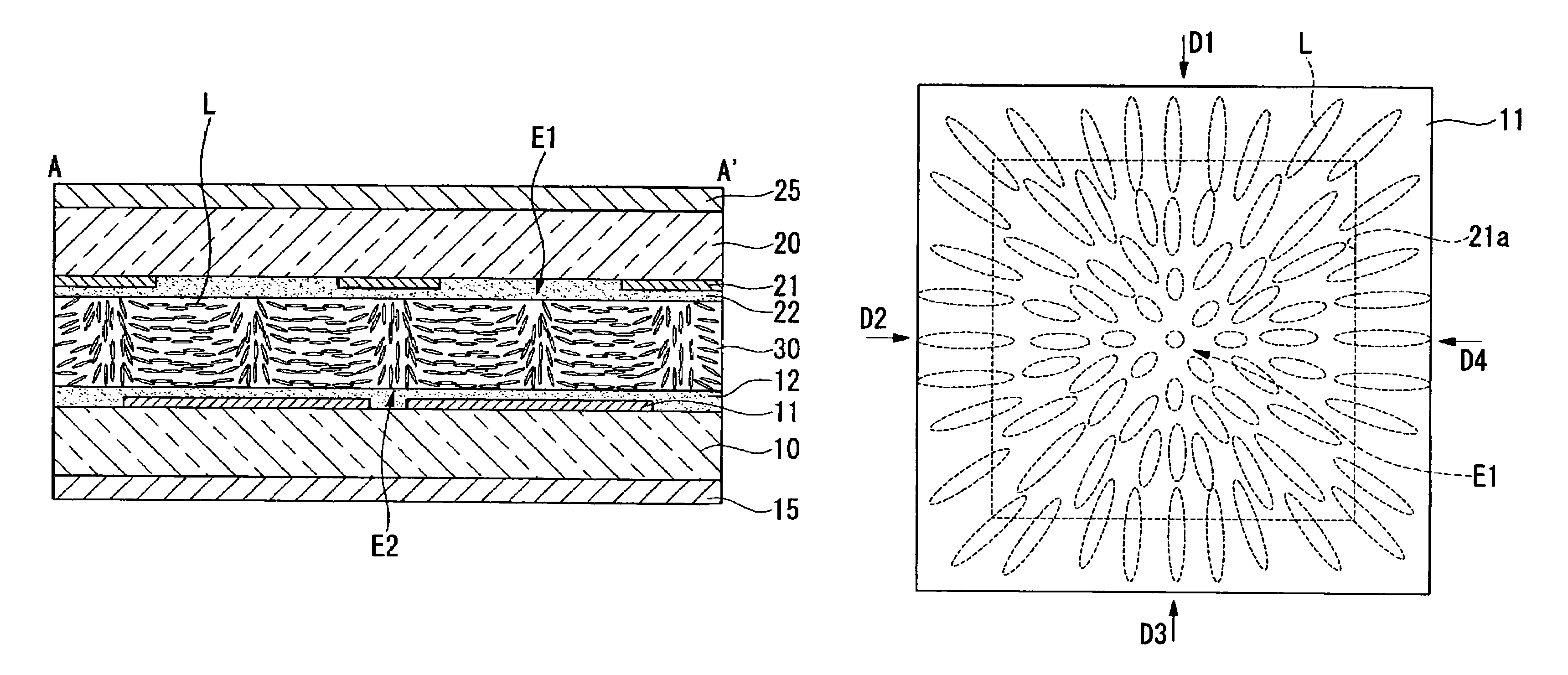
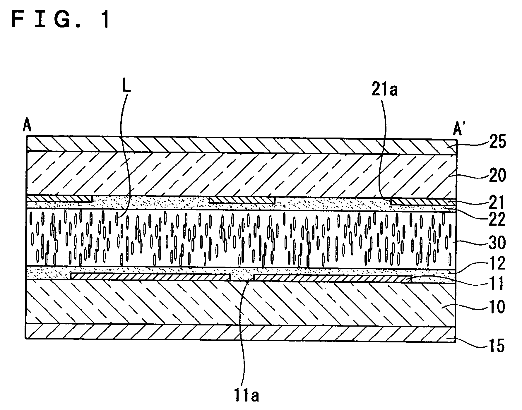
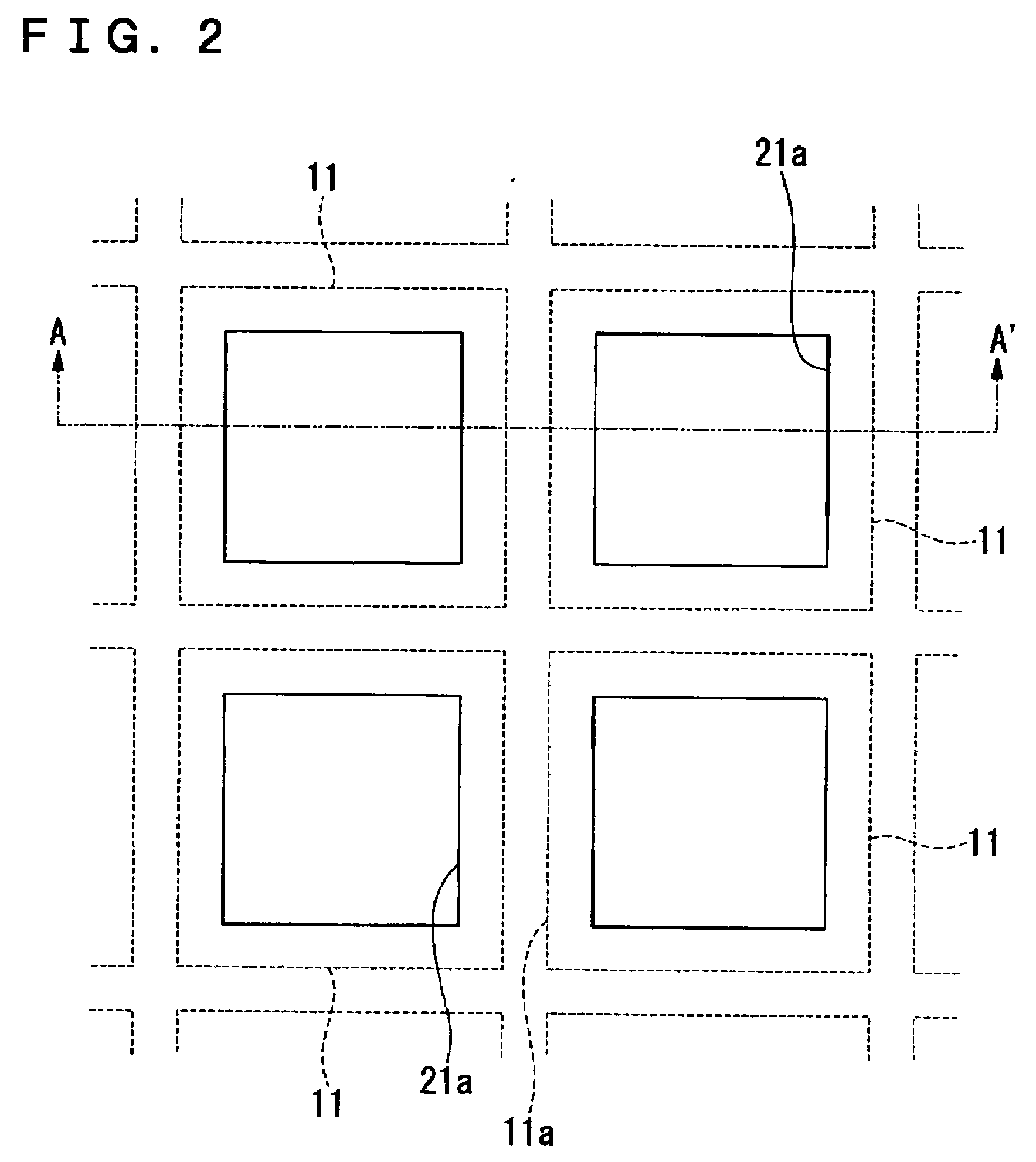
[0029]Referring now to FIG. 1 to FIG. 4, a liquid crystal device according to a first exemplary embodiment of the present invention will be described. FIG. 1 is a cross-sectional schematic showing a structure of the liquid crystal device according to the present exemplary embodiment. FIG. 2 is a schematic of a principal structure thereof when viewed from the side of the opposed substrate, FIG. 3 is a schematic showing a state of alignment of the liquid crystal when a voltage is applied. FIG. 4 is a schematic showing a state of alignment of the liquid crystal in one pixel. In these drawings, contraction scales of the layers or members are different from each other in order to make these layers or members recognizable in the drawings. In this specification, in each member constituting the liquid crystal device, the surface disposed on the side of the liquid crystal layer is referred to as “inner surface” and the opposite surface therefrom is referred to as “outer surface”.

[0030]T...

second exemplary embodiment

[0040

[0041]Referring now to FIG. 5 and FIG. 6, the liquid crystal device according to a second exemplary embodiment of the present invention will be described. In the present embodiment, the same parts as in the aforementioned first exemplary embodiment are represented by the same reference numerals, and will not be described here.

[0042]The present exemplary embodiment is a modification in structure of the aforementioned first exemplary embodiment, in which the shape of the pixel electrode and the shape of the opening of the light shielding film are modified. In other words, as shown in FIG. 5, a pixel electrode 11′ in the present exemplary embodiment has an octagonal shape with the corners of the pixel electrode 11 in the aforementioned first exemplary embodiment cut off, and the light shielding film is formed with octagonal openings 21a′ correspondingly. The shape of the pixel electrode 11′ and the shape of the openings of the light shielding film may be a polygon having no acute-...

third exemplary embodiment

[0044

[0045]Referring now to FIG. 7, the liquid crystal device according to a third exemplary embodiment of the present invention will be described. In the present exemplary embodiment, the same parts as in the aforementioned first exemplary embodiment are represented by the same reference numerals and will not be described here.

[0046]In the present exemplary embodiment of the invention, chiral material is added to a liquid crystal layer 30′. Hence alignment of the liquid crystal molecules L can be controlled more stably. In the liquid crystal device of a homeotropic alignment type described above, the liquid crystal molecules L fall down in the state of being twisted in predetermined directions when a voltage is applied. The twisting directions are not constant, but are unstable. Hence the twisting directions of the liquid crystal molecules are random among different pixels, although the twisting directions are the same in the same pixel. When the plurality of domains being differen...


PUM

PropertyMeasurementUnit
voltageaaaaaaaaaa
negative dielectric anisotropyaaaaaaaaaa
electric fieldaaaaaaaaaa

Abstract

To achieve clear image display without providing a feeling of roughness by fixing the position where disclination is generated in a liquid crystal device of a homeotropic alignment type, a conductive light shielding film provided on the side of an opposed substrate as a common electrode to drive a liquid crystal layer by pixel electrodes of an array substrate and the light shielding film of the opposed substrate.

Description

BACKGROUND OF THE INVENTION[0001]1. Field of Invention[0002]The present invention relates to a liquid crystal device and electronic equipment provided with the same and specifically, to an alignment control technology for a fine homeotropic alignment liquid crystal device suitable for being used in a light bulb in a projector, in a display unit of a mobile phone or a PDA, and so on.[0003]2. Description of Related Art[0004]A display of high-contrast and wide angle of visibility is required in the field of liquid crystal devices. A homeotropic alignment mode is presently being studied to realize such a display. A liquid crystal device of a homeotropic alignment type has a structure in which liquid crystal having negative dielectric anisotropy is enclosed between a pair of opposed substrates. One of these substrates is configured, for example, as an array substrate having a plurality of pixel electrodes arranged in a matrix manner and a TFT for switching each pixel electrode individual...

Claims


Application Information

Patent Timeline
Patent Type & Authority Patents(United States)
IPC IPC(8): G02F1/1333G02F1/1335G02F1/1337G02F1/1343G02F1/139
CPCG02F1/133512G02F1/1393G02F1/133707G02F2001/133742G02F1/133742F25B30/02F25B47/006F25B2700/2103
Inventor OKAZAKI, TSUYOSHIOZAWA, KINYAMAEDA, TSUYOSHI
Owner 138 EAST LCD ADVANCEMENTS LTD
Learn More