Printed circuit board

a printed circuit board and circuit board technology, applied in the direction of printed element electric connection formation, high frequency circuit adaptation, electrical apparatus construction details, etc., can solve the problems of electromagnetic noise radiating from various types of electronic devices such as information devices, loss when signals pass through plural layers through via holes,

Active Publication Date: 2006-12-12
FUJIFILM BUSINESS INNOVATION CORP
View PDF6 Cites 20 Cited by
  • Summary
  • Abstract
  • Description
  • Claims
  • Application Information

AI Technical Summary

Benefits of technology

[0017]The present invention has been made in view of the above circumstances and provides a low-cost printed circuit board which can suppress electromagnetic radiation such as common mode radiation.

Problems solved by technology

It is known that dielectric loss and the skin effect impede the transmission of signals of a GHz order on a printed circuit board.
Moreover, loss when the signals pass through plural layers through via holes for interconnecting different plural layers in a multilayer board also cannot be ignored.
Also, when the return current cannot flow through the reference surfaces, a distant electromagnetic field is not cancelled due to the return current being incomplete.
Electromagnetic noise radiating from various types of electronic devices such as information devices, which has conventionally been a problem, is thought to result mainly from the signal wires of clock signals on the printed circuit board and digital signals synchronized with the clock signals.
The affect of common mode radiation resulting from the return current being cut off is also large.
In other words, it was understood that transmission of a GHz order in such a case is hardly practical.
However, even in a case where a connection-use via hole is disposed in the vicinity of a signal-use via hole (e.g., a distance of 1.5 mm), the return current does not return in a GHz order and the effect of the improvement is small.

Method used


Image

  • Printed circuit board
  • Printed circuit board
  • Printed circuit board

Examples


first embodiment

[0063]the invention will be described below.

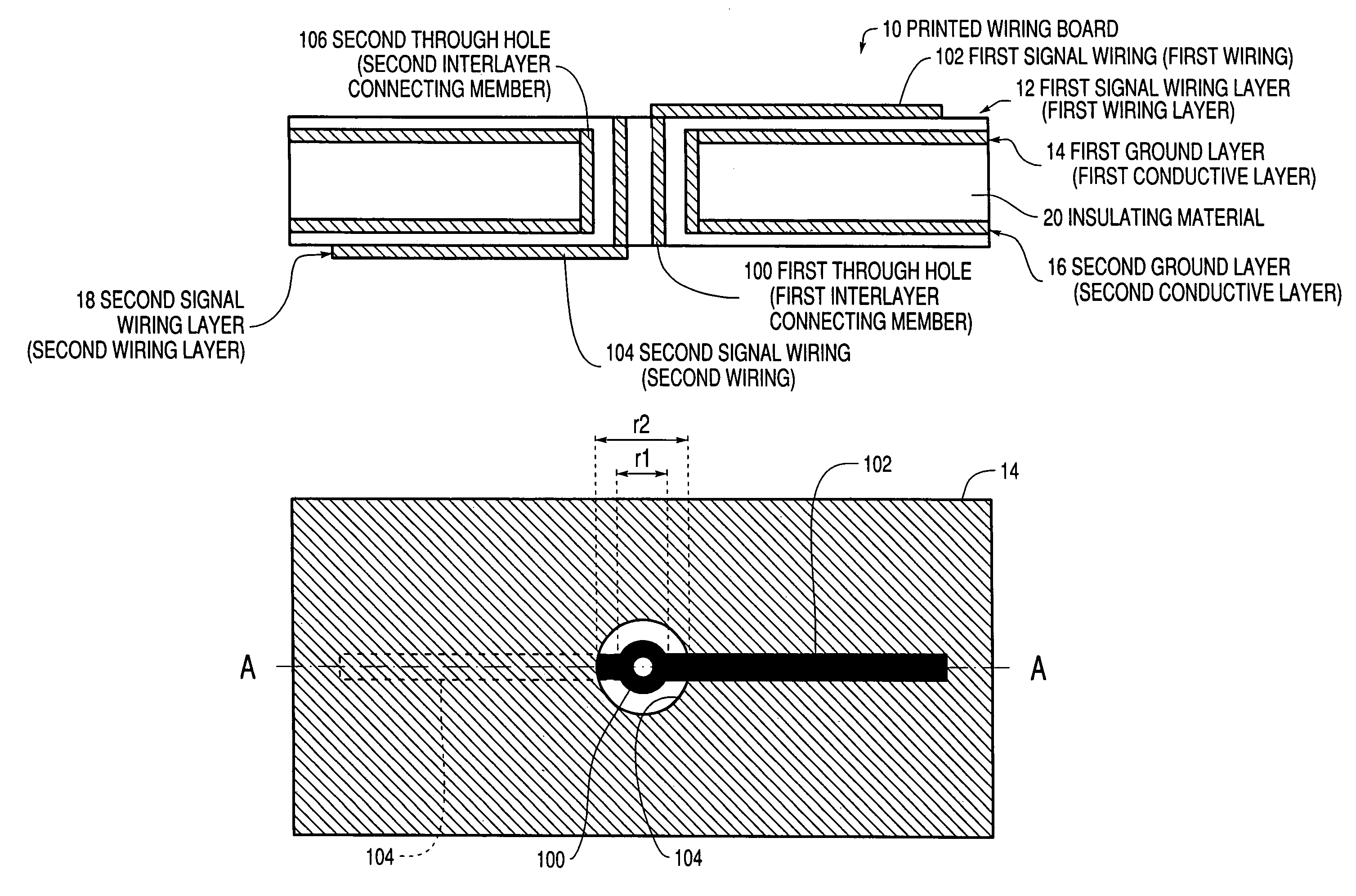
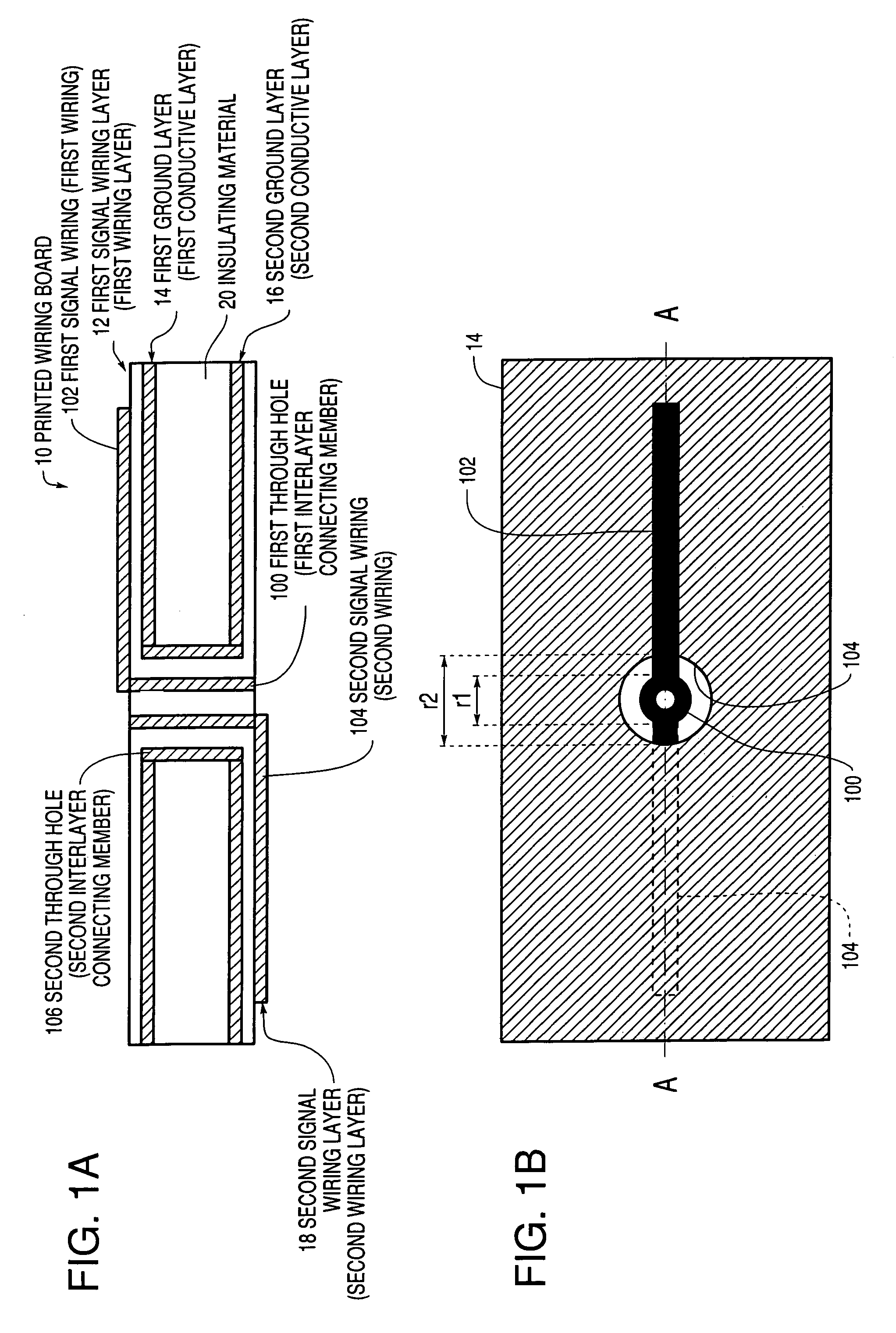
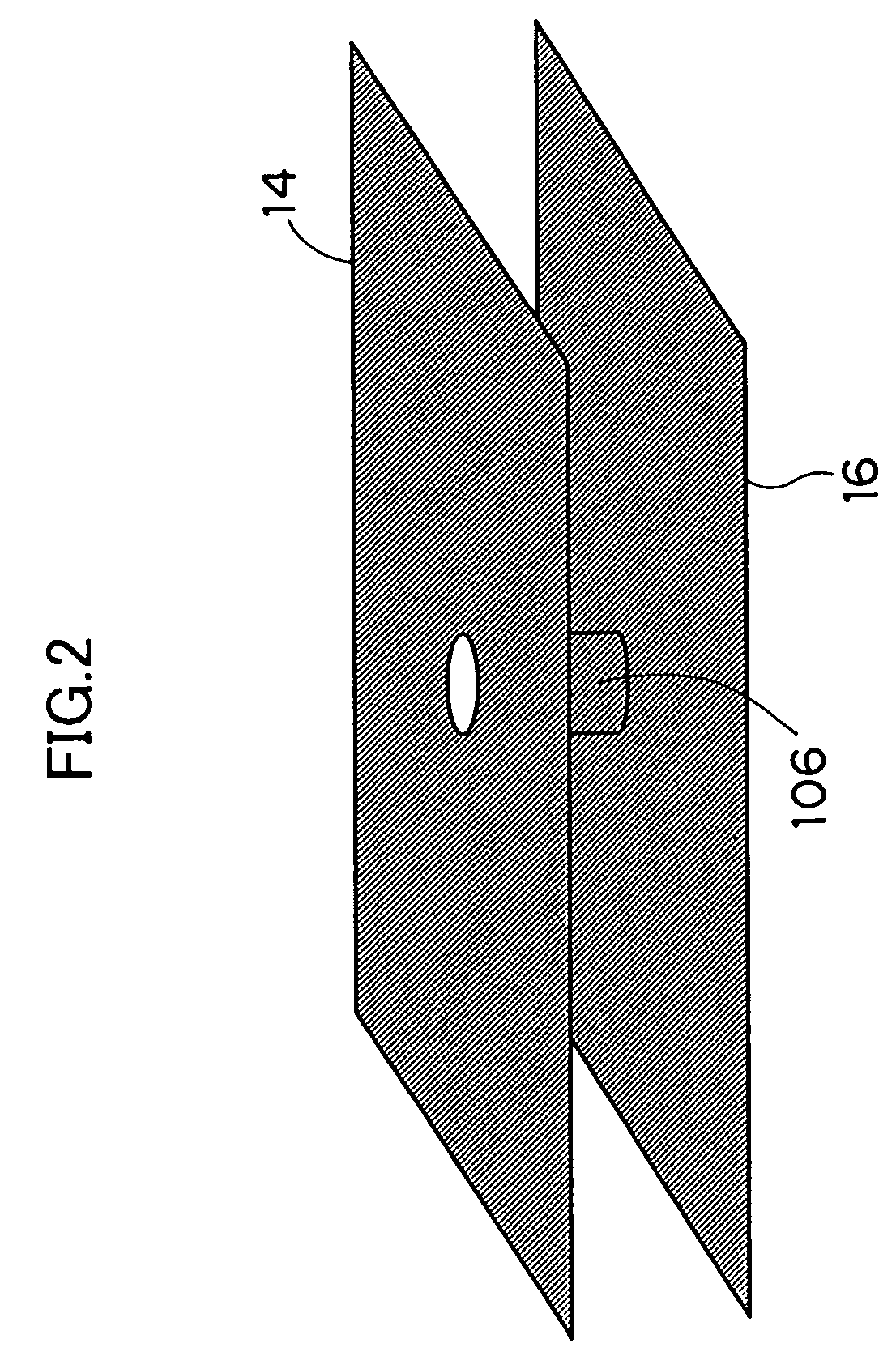
[0064]FIG. 1A shows a schematic cross-sectional view of a printed circuit board 10 according to the present embodiment. As shown in FIG. 1A, the printed circuit board 10 includes a 4-layer board of a multilayer structure where a first signal wiring layer 12, a first ground layer 14, a second ground layer 16 and a second signal wiring layer 18 are laminated via an insulating material 20.

[0065]FIG. 1B shows a plan view of the first ground layer 14. It should be noted that the insulating material 20 is omitted for ease of description. Also, FIG. 1A is a cross-sectional view along line A—A of FIG. 1B.

[0066]As shown in FIG. 1A, a cylindrical conductive first through hole 100 is disposed in the printed circuit board 10. A conductive first signal wiring 102 is formed on the first signal wiring layer 12 and a conductive second signal wiring 104 is formed on the second signal wiring layer 18. The signal wiring 102 and the signal wiring 104 are conn...

third embodiment

[0094]Next, the invention will be described. It should be noted that the same reference numerals will be given to portions that are identical to those of the preceding embodiments and that detailed description of those portions will be omitted.

[0095]FIG. 5 shows a schematic cross-sectional view of a printed circuit board 120 according to the present embodiment.

[0096]As shown in FIG. 5, the printed circuit board 120 includes a BGA (Ball Grid Array) type IC 122 mounted on the first signal wiring layer 12. A power wiring 126 to which power pins 124 of the IC 122 are connected is connected is to one end portion of the first through hole 100, and the other end portion of the first through hole 100 is connected to a power wiring 128 formed on the second signal wiring layer 18. Namely, power is supplied to the IC 122 via the first through hole 100 from the power wiring 128 formed on the second signal wiring layer 18. Additionally, the first through hole 100 is surrounded by the second thro...

fourth embodiment

[0107]Next, the invention will be described. It should be noted that the same reference numerals will be given to portions that are identical to those of the preceding embodiments and that detailed description of those portions will be omitted. In the present embodiment, an embodiment of a printed circuit board in a case where a differential signal outputted from a differential signal driver is outputted from the first signal wiring layer 12 side to the second signal wiring layer 18 side will be described.

[0108]FIG. 10 shows a partial perspective view of a printed circuit board 150 according to the present embodiment. For ease of description, FIG. 10 shows only the first ground layer 14, the second ground layer 16, a differential signal driver 152 mounted on the first signal wiring layer 12, a pair of differential signal-use wirings 154A and 154B wired to the first signal wiring layer 12, a pair of first through holes 100A and 100B, the second through hole 106, and a pair of differe...


PUM


Abstract

In a printed circuit board of the invention, a first signal wiring layer, a first ground layer, a second ground layer and a second signal wiring layer are laminated via an insulating material. A first signal wiring is formed on the first signal wiring layer and a second signal wiring is formed on the second signal wiring layer. The two signal wirings are connected via a first through hole. The conductive first ground layer and the conductive second ground layer are connected via a second through hole. The second through hole is insulated from the first through hole and formed so as to surround the first through hole.

Description

CROSS-REFERENCE TO RELATED APPLICATION[0001]This application claims priority under 35 USC 119 from Japanese Patent Application No. 2003-119960, the disclosures of which are incorporated by reference herein.BACKGROUND OF THE INVENTION[0002]1. Field of the Invention[0003]The present invention relates to a printed circuit board, and in particular to a printed circuit board used in electronic devices such as, for example, personal computers, copiers, printers and fax machines.[0004]2. Description of the Related Art[0005]In order to transmit digital signals on printed circuit boards used in electronic devices, it is necessary to be able to sufficiently transmit digital signals with harmonic waves of ordinarily up to five times or greater with respect to the frequency of fundamental waves of a binary pulse. Namely, in order to transmit high-speed digital signals whose base clock is several hundred MHz or greater, consideration must be given to harmonic components of a GHz order.[0006]It i...

Claims


Application Information

Patent Timeline
Patent Type & Authority Patents(United States)
IPC IPC(8): H05K7/02H05K7/06H05K7/08H05K7/10H05K3/46H01L23/12H05K1/02H05K1/11H05K1/16H05K3/34H05K3/42
CPCH05K1/0222H05K1/0251H05K1/115H05K1/162H01L24/16H05K1/0231H05K1/0245H05K3/3447H05K3/429H05K2201/09236H05K2201/093H05K2201/09336H05K2201/0949H05K2201/09636H05K2201/09663H05K2201/09809H05K2201/10689H05K2201/10734H01L2224/16225H01L2924/12042H01L2924/00014H01L2924/00H01L2224/0401
Inventor IGUCHI, DAISUKE
Owner FUJIFILM BUSINESS INNOVATION CORP
Why Eureka
Try Eureka