Mobile communication terminal device and variable gain circuit

Inactive Publication Date: 2006-12-12
SONY ERICSSON MOBILE COMM JAPAN INC
View PDF8 Cites 42 Cited by
  • Summary
  • Abstract
  • Description
  • Claims
  • Application Information

AI Technical Summary

Benefits of technology

[0015]In view of the above-mentioned problems with the related art, the present invention aims at providing a mobile communication terminal device and variable gain circuit that ensur

Problems solved by technology

Normal operation of the PGA circuit cannot be expected during this saturated state.
If the cutoff frequency is not set to an extremely low value, then a lack of low frequency components in the input-to-output signal transfer characteristics will increase to a level that is not acceptable for baseband amplifiers.
This creates the problem that time (DC voltage converge

Method used


Image

  • Mobile communication terminal device and variable gain circuit
  • Mobile communication terminal device and variable gain circuit
  • Mobile communication terminal device and variable gain circuit

Examples


first embodiment

[0029][First Embodiment]

[0030]The present invention can be applied to cellular phones compatible with the W-CDMA (DS-CDMA: Direct Spread Code Division Multiple Access) method.

[0031][Overview of signal processing in cellular phones]

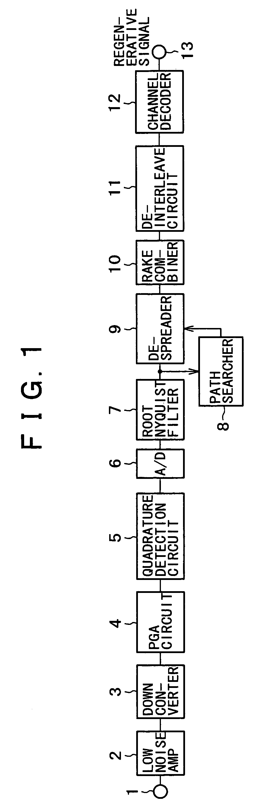
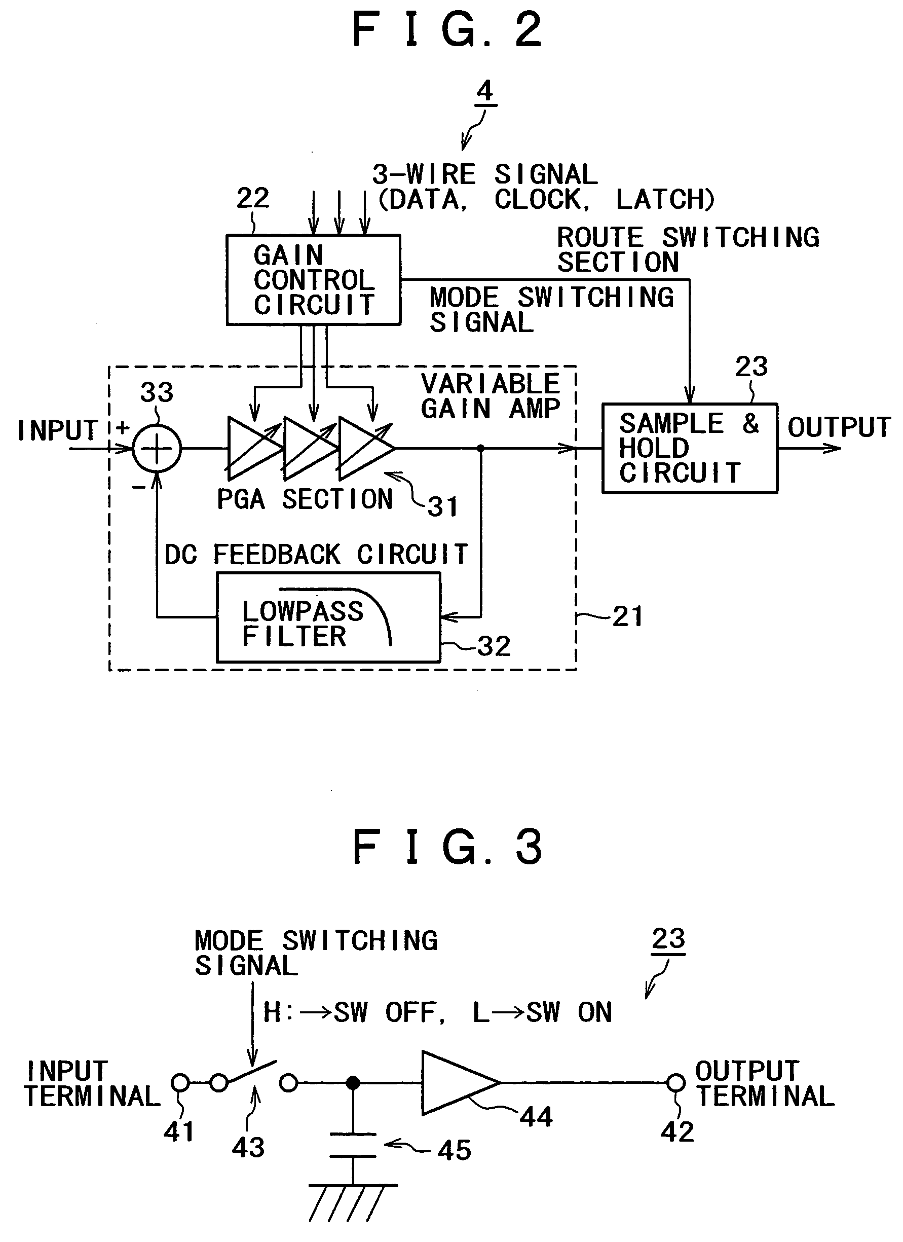
[0032]FIG. 1 is a block diagram showing the cellular phone receiver system of a first embodiment of the present invention. As this figure shows, the signal received by an antenna is first amplified by a low-noise amplifier 2 via an input terminal 1. The amplified signal is then linearly amplified by a programmable gain amplifier (PGA) 4 after being converted to an intermediate frequency (IF frequency) by a down converter 3.

[0033]This linearly amplified received signal is processed by a quadrature detection circuit 5 and separated into an in-phase component and a quadrature component. The separated components are respectively converted into digital signals by an A / D converter 6. These digitalized in-phase components and quadrature components are passed thro...

second embodiment

[0059][Second Embodiment]

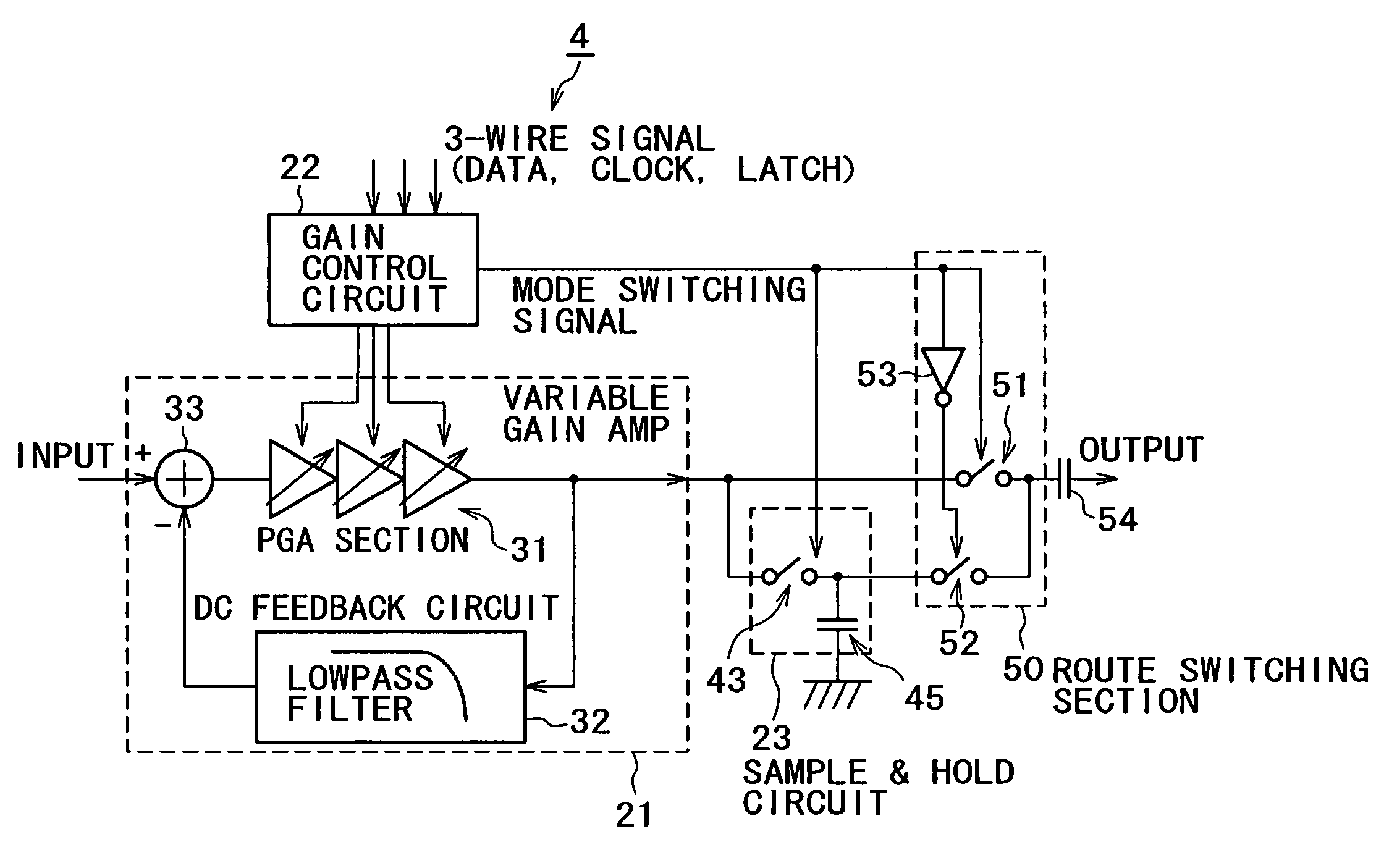
[0060]The second embodiment of the present invention is described next with another cellular phone. In this cellular phone of the second embodiment, the PGA circuit 4 comprises a path switching section 50 for switching between the output from the sample-and-hold circuit 23 and the output from the variable gain amplifier 21 as shown in FIG. 6.

[0061]The only point differing from the first embodiment is that the second embodiment contains this path switching section 50. The operations of all other sections are identical to those for the first embodiment so only the operation of the path switching section 50 is described to avoid redundant description.

[0062]The path switching section 50 installed into the PGA circuit 4 in the cellular phone of the second embodiment has a first selector switch 51 that turns the output signal from the variable gain amplifier 21 on or off and a second selector switch 52 that turns the output signal from the sample-and-hold circuit ...


PUM


Abstract

In receiver systems for cellular phones using the W-CDMA method, the change in DC voltage occurring when the gain of a programmable gain amplifier (PGA circuit) is switched to adjust the gain for a received signal, can be suppressed. A sample-and-hold circuit is installed containing a “sample” mode for directly outputting a signal from the PGA section and also containing a “hold” mode for outputting the electric charge of a specified voltage stored in a capacitor. This sample-and-hold circuit normally operates in “sample” mode so the output signal from the PGA section is directly output, but is operated in “hold” mode at the gain switching timing of the PGA circuit, so that the electric charge of the specified voltage stored in the capacitor is output for a specified length of time (equal to the time required for the DC voltage change to converge to a stable level).

Description

BACKGROUND OF THE INVENTION[0001]1. Field of the Invention[0002]The present invention relates to a mobile communication terminal device and a variable gain circuit that is preferably installed, for example, in cellular phones compatible with the W-CDMA (Wideband-Code Division Multiple Access) method, PHS (Personal Handyphone System) phones or PDA (Personal Digital(Data) Assistants) having wireless communication capability.[0003]2. Description of Related Art[0004]The received power level distribution of antennas used in modern cellular phones spans a wide range from 80 dB to 100 dB. To cope with this, cellular phone receivers use an automatic gain control circuit (AGC circuit) that adjusts the signals received over this wide range to an optimum level so that the appropriate signals are transferred to the baseband A / D converter.[0005]Analog control type circuits (VGA circuit: voltage-controlled gain amplifier) have been commonly used as AGC circuits to adjust the voltage serving as th...

Claims


Application Information

Patent Timeline
IPC IPC(8): H04B1/06H03G1/04H03G3/10H03G3/20H04B1/10
CPCH03G3/3078H04B1/109
Inventor YOSHIZAWA, ATSUSHI
Owner SONY ERICSSON MOBILE COMM JAPAN INC
Why Eureka
Try Eureka