Semiconductor chip package

Active Publication Date: 2006-12-19
ADVANCED SEMICON ENG INC
View PDF6 Cites 4 Cited by
  • Summary
  • Abstract
  • Description
  • Claims
  • Application Information

AI Technical Summary

Benefits of technology

[0007]It is an object of the present invention to provide a high-pin-count BGA package which allows the stresses on the solder balls located i

Problems solved by technology

Integrated circuit (chip) packaging technology is becoming a limiting factor for the development in packaged integrated circuits of higher performance.
Semiconductor package designers are struggling to keep pace with the increase in pin count, size limitations, low profile mounting constraints, and other evolving requirements for packaging and mounting integrated circuits.
Any BGA package that utilizes solder balls to electrically couple the packaged integrated circuit to a main PCB is susceptible to failure, particularly fatigue failure, due to temperature fluctuations and dissimilarity in thermal expansion rates for the components that form the BGA package.
Specifically, as the BGA package cools down from the solder reflow temperature or undergoes ambient temperature changes during use, the BGA package experiences thermal deformation of diff

Method used


Image

  • Semiconductor chip package
  • Semiconductor chip package
  • Semiconductor chip package

Examples


Embodiment Construction

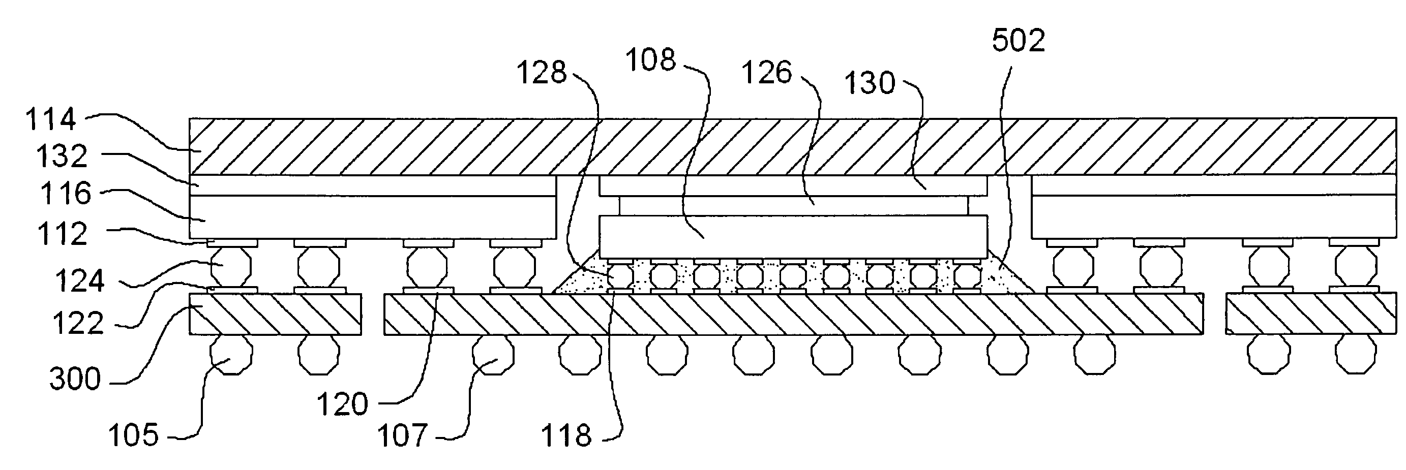
[0027]FIG. 1 illustrates a semiconductor chip package 100 according to one embodiment of the present invention. The semiconductor chip package 100 generally includes an interconnection substrate 102, a central substrate 104, a peripheral substrate 106, a semiconductor chip 108, a plurality of central solder balls 105 disposed on the bottom surface of the central substrate 104 and a plurality of peripheral solder balls 107 disposed on the bottom surface of the peripheral substrate 106. The peripheral substrate 106 has an opening 106a, and the central substrate 104 is disposed in the opening 106a of the peripheral substrate and substantially coplanar with the peripheral substrate 106.

[0028]The bottom surface of the interconnection substrate 102 has a recessed cavity 110 defined therein and a plurality of contact pads 112 formed around the recessed cavity 110. The interconnection substrate 102 may include a top plate 114, preferably a heat-sink, and a dielectric layer 116. The dielectr...


PUM


Abstract

A semiconductor chip package includes an interconnection substrate, a central substrate, a peripheral substrate and a semiconductor chip sandwiched between the interconnection substrate and the central substrate. The interconnection substrate has a recessed cavity for receiving the semiconductor chip. The peripheral substrate is separated from the central substrate thereby decreasing the stresses caused by CTE mismatch of the semiconductor chip package. Furthermore, both the central substrate and the peripheral substrate are mechanically and electrically connected to the interconnection substrate such that the semiconductor chip is electrically connected to the peripheral substrate through the central substrate and the interconnection substrate.

Description

BACKGROUND OF THE INVENTION[0001]1. Field of the Invention[0002]This invention generally relates to a semiconductor chip package and the method for making the same.[0003]2. Description of the Related Art[0004]Integrated circuit (chip) packaging technology is becoming a limiting factor for the development in packaged integrated circuits of higher performance. Semiconductor package designers are struggling to keep pace with the increase in pin count, size limitations, low profile mounting constraints, and other evolving requirements for packaging and mounting integrated circuits. Currently, the common packaging and package mounting technology is a ball grid array (BGA) package, in which an array of solder pads for solder balls are formed on the integrated circuit package. Conductive leads or traces on the package connect the solder pads to wire bonding pads for electrically connection to the integrated circuit chip within the package. A corresponding array of solder pads is formed on ...

Claims


Application Information

Patent Timeline
IPC IPC(8): H01L23/58H01L23/36H01L23/498
CPCH01L23/36H01L23/49816H01L23/49833H01L2224/32225H01L2924/07811H01L2924/15311H01L2924/01079H01L23/49838H01L2224/16225H01L2224/73204H01L2224/73253H01L2924/00H01L2224/05568H01L2224/05573H01L2924/00014H01L2224/05599
Inventor TAO, SULEE, SHIH CHANG
Owner ADVANCED SEMICON ENG INC
Why Eureka
Try Eureka