Spontaneous light emitting display device

Inactive Publication Date: 2006-12-26
RAKUTEN GRP INC
View PDF15 Cites 72 Cited by
  • Summary
  • Abstract
  • Description
  • Claims
  • Application Information

AI Technical Summary

Benefits of technology

[0015]According to such a structure, it is possible to produce an effect that

Problems solved by technology

Consequently, there is a problem that unnecessary light e

Method used


Image

  • Spontaneous light emitting display device
  • Spontaneous light emitting display device
  • Spontaneous light emitting display device

Examples


embodiment 1

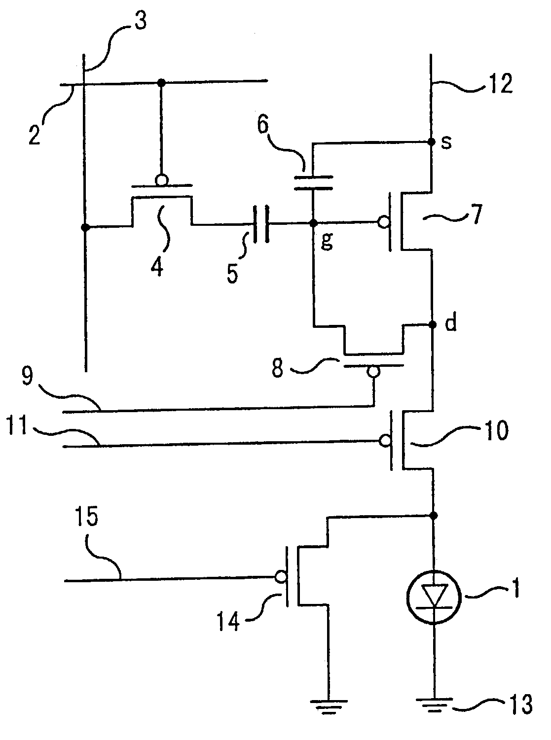
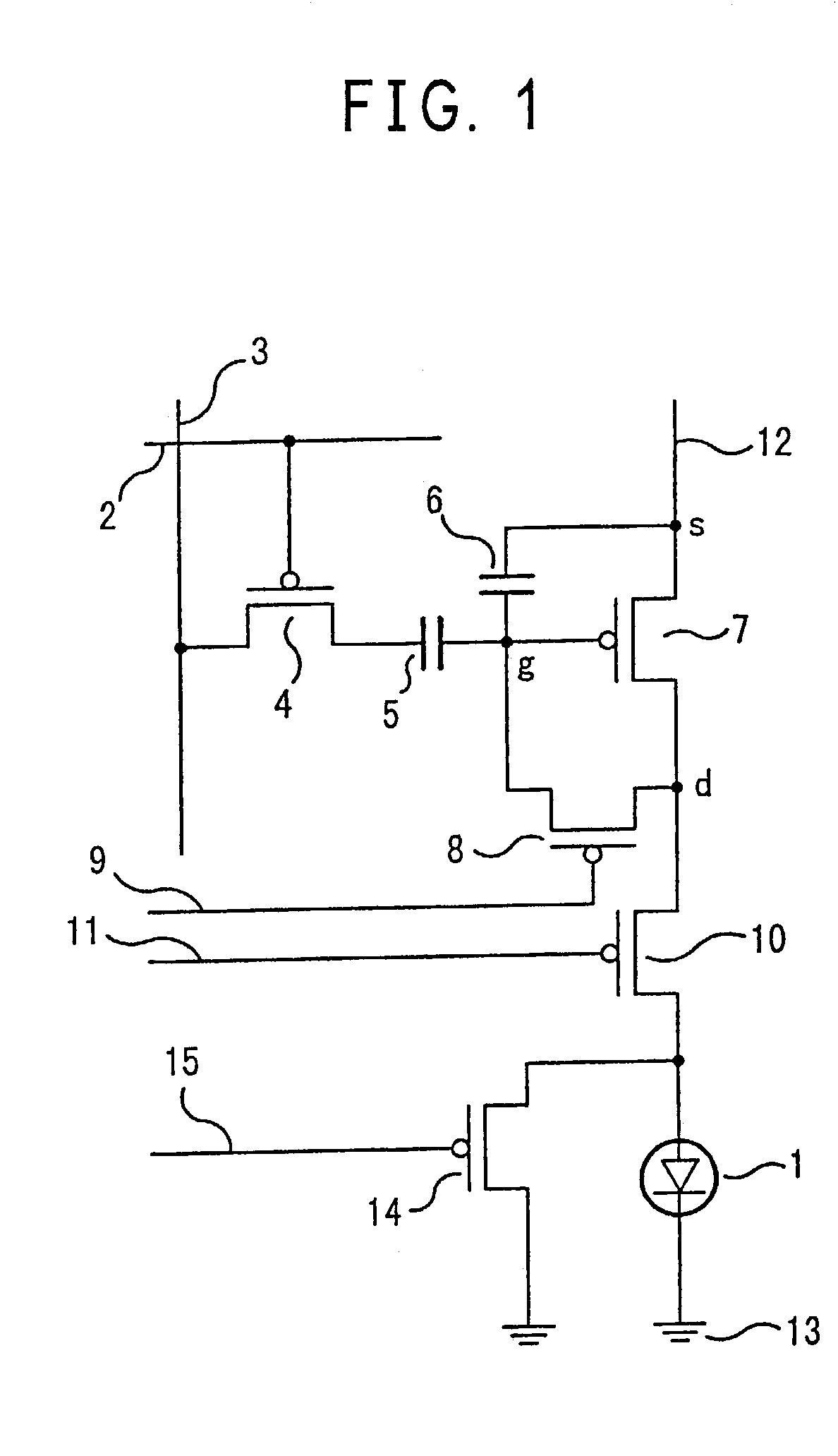
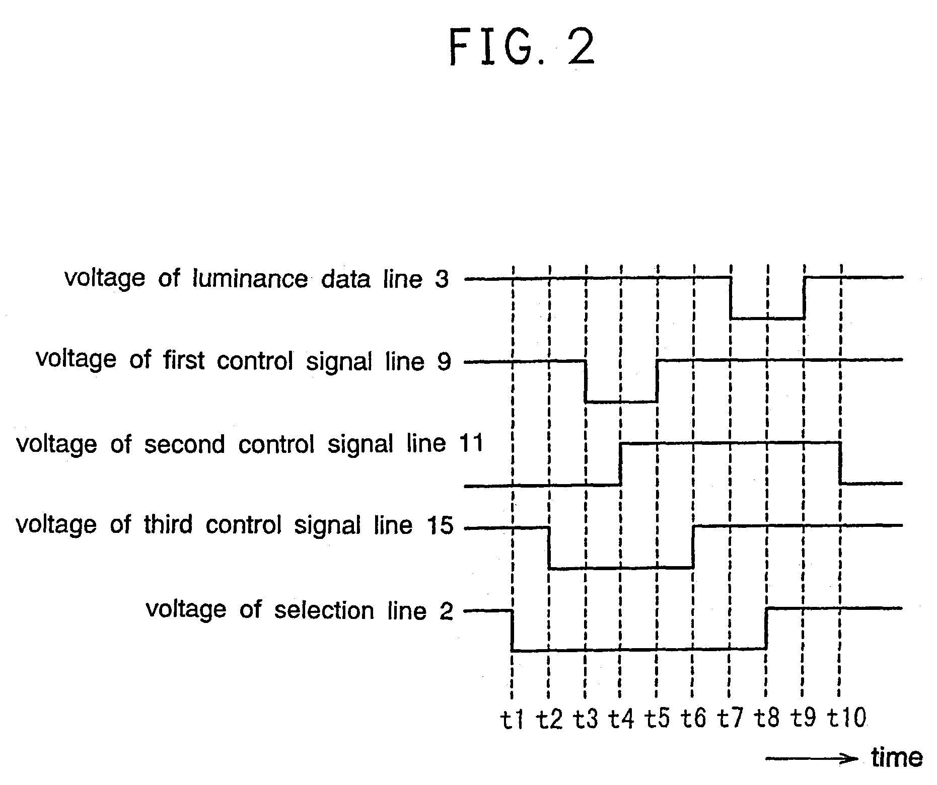
[0027]FIGS. 1 and 2 are circuit and waveform diagrams showing a driving circuit and a timing for explaining means for suppressing a noise current according to Embodiment 1 of the present invention. More specifically, FIG. 1 is a circuit diagram showing a driving circuit in the case in which a transistor is applied as a switching element and all the transistors are P channel FETs, and FIG. 2 is a waveform diagram showing the operation timing of each signal voltage in FIG. 1. In FIG. 1, reference numerals 1 to 13 indicate the same components as those in FIG. 9. Reference numeral 14 denotes a fifth transistor to be a P channel FET which is connected in parallel with an organic electroluminescence element 1, and reference numeral 15 denotes a third control signal line for supplying a signal voltage to control the fifth transistor 14 into a conduction or non-conduction state. For the luminance data writing period of the driving circuit in the same figure, the transistor 14 is conducted f...

embodiment 2

[0030]FIG. 3 is a circuit diagram for explaining a driving circuit for suppressing a noise current according to Embodiment 2 of the present invention. In FIG. 3, the third control signal line 15 and the selection line 2 in FIG. 1 are shared. The driving circuit shown in FIG. 3 is operated based on a waveform diagram for explaining an operation timing of FIG. 10. A fifth transistor 14 is conducted for a period in which a pixel is selected, and moreover for a period from a time before a third transistor 8 is brought into a conduction state to a time after a fourth transistor 10 is brought into a non-conduction state. Therefore, the same effects as those in Embodiment 1 can be obtained. Furthermore, it is possible to obtain an effect that the number of the signal lines is decreased and a circuit structure can be thereby prevented from being complicated.

embodiment 3

[0031]FIG. 4 is a circuit diagram for explaining a driving circuit to suppress a noise current according to Embodiment 3 of the present invention. In FIG. 4, the third control signal line 15 and the first control signal line 9 in FIG. 1 are shared. The driving circuit in FIG. 4 is operated based on a waveform diagram for explaining an operation timing of FIG. 10. A fifth transistor 14 is conducted for a period in which a pixel is selected, and moreover for a period from a time before a third transistor 8 is brought into a conduction state to a time after a fourth transistor 10 is brought into a non-conduction state. Therefore, the same effects as those in Embodiment 1 can be obtained. Furthermore, it is possible to obtain an effect that the number of the signal lines is decreased and a circuit structure can be thereby prevented from being complicated.


PUM


Abstract

In a driving circuit of a spontaneous light emitting display device driven as an active matrix, a noise current is prevented from flowing in a light emitting element when compensating for a threshold voltage of a transistor for controlling current flowing to the emitting element, enhancing precision in luminance. A switching element for short-circuiting electrodes of the spontaneous light emitting element for a period in which the noise current flows in the light emitting element bypasses the noise current.

Description

TECHNICAL FIELD[0001]The present invention relates to a luminance control for a spontaneous light emitting element in a spontaneous light emitting display device using an active matrix method.BACKGROUND ART[0002]FIG. 7 shows a conventional driving circuit corresponding to one pixel of a spontaneous light emitting type display device using an active matrix method which has been disclosed in the cited reference ‘T. P. Brody, et al., “A 6×6—in 20-1 pi Electroluminescent Display Panel”, IEEE Trans. on Electron Devices, Vol. ED-22, No. 9, pp. 739–748 (1975)”’. Tr1 denotes the first transistor which operates as a switching element. Tr2 denotes the second transistor which operates as a driving element for controlling the current of a spontaneous light emitting element. C1 denotes a capacitor connected to the drain terminal of the first transistor Tr1. A spontaneous light emitting element 60 is connected to the drain terminal of the second transistor Tr2. Next, an operation will be describe...

Claims


Application Information

Patent Timeline
IPC IPC(8): G09G3/30G09G3/10G09G3/20H01L51/50G09G3/32H05B33/14
CPCG09G3/3233G09G2300/0819G09G2300/0852G09G2300/0861G09G2310/06G09G2320/0233G09G2320/043G09G3/30
Inventor OKABE, MASASHIINOUE, MITSUOIWATA, SHUJIYAMAMOTO, TAKASHI
Owner RAKUTEN GRP INC
Why Eureka
Try Eureka