Clock signal initiated precharge technique for active memory subarrays in dynamic random access memory (DRAM) devices and other integrated circuit devices incorporating embedded DRAM

a technology of dynamic random access memory and precharge technique, which is applied in the direction of information storage, static storage, digital storage, etc., can solve the problems of discharging leakage power and down memory access, and achieve the effect of reducing the clock period and improving logi

Inactive Publication Date: 2006-12-26
SONY CORP
View PDF9 Cites 6 Cited by
  • Summary
  • Abstract
  • Description
  • Claims
  • Application Information

AI Technical Summary

Benefits of technology

[0007]In accordance with the technique of the present invention as disclosed herein, the rising edge of each clock initiates a precharge to those memory subarrays that were active. This differs from conventional approaches wherein the subarrays are typically precharged such that they are made ready on the rising edge of the clock, which would then start an active cycle. The longer restore time can be used to achieve the introduction of better logic “1” and “0” levels into the memory cell and / or to reduce the clock period.
[0008]The technique of the present invention provides a number of advantages over conventional techniques, among which are that: a) a timer may be used to determine the end of a precharge operation rather than the end of a cell restore function. The former is a shorter time period and, therefore, an easier timer function to implement; b) faster clock frequencies can be achieved; c) by starting each clock cycle with a precharge command, other functions can be performed in parallel with the precharge function (for example, address pre-decoding, data propagation for write functions and, in a particular embodiment of the present invention, the access to determine a cache “hit” or “miss”. This parallel operation allows for less “dead” time and overall higher performance); and d) further, the amount of time used to restore voltage into the DRAM array memory cell can be changed with longer or shorter clock periods.

Problems solved by technology

However, the technique described employs an activity monitor circuit in series with the address path which appreciably slows down memory accesses.
Moreover, the memory arrays can remain active for relatively long periods of time thereby dissipating leakage power.

Method used


Image

  • Clock signal initiated precharge technique for active memory subarrays in dynamic random access memory (DRAM) devices and other integrated circuit devices incorporating embedded DRAM
  • Clock signal initiated precharge technique for active memory subarrays in dynamic random access memory (DRAM) devices and other integrated circuit devices incorporating embedded DRAM
  • Clock signal initiated precharge technique for active memory subarrays in dynamic random access memory (DRAM) devices and other integrated circuit devices incorporating embedded DRAM

Examples


Embodiment Construction

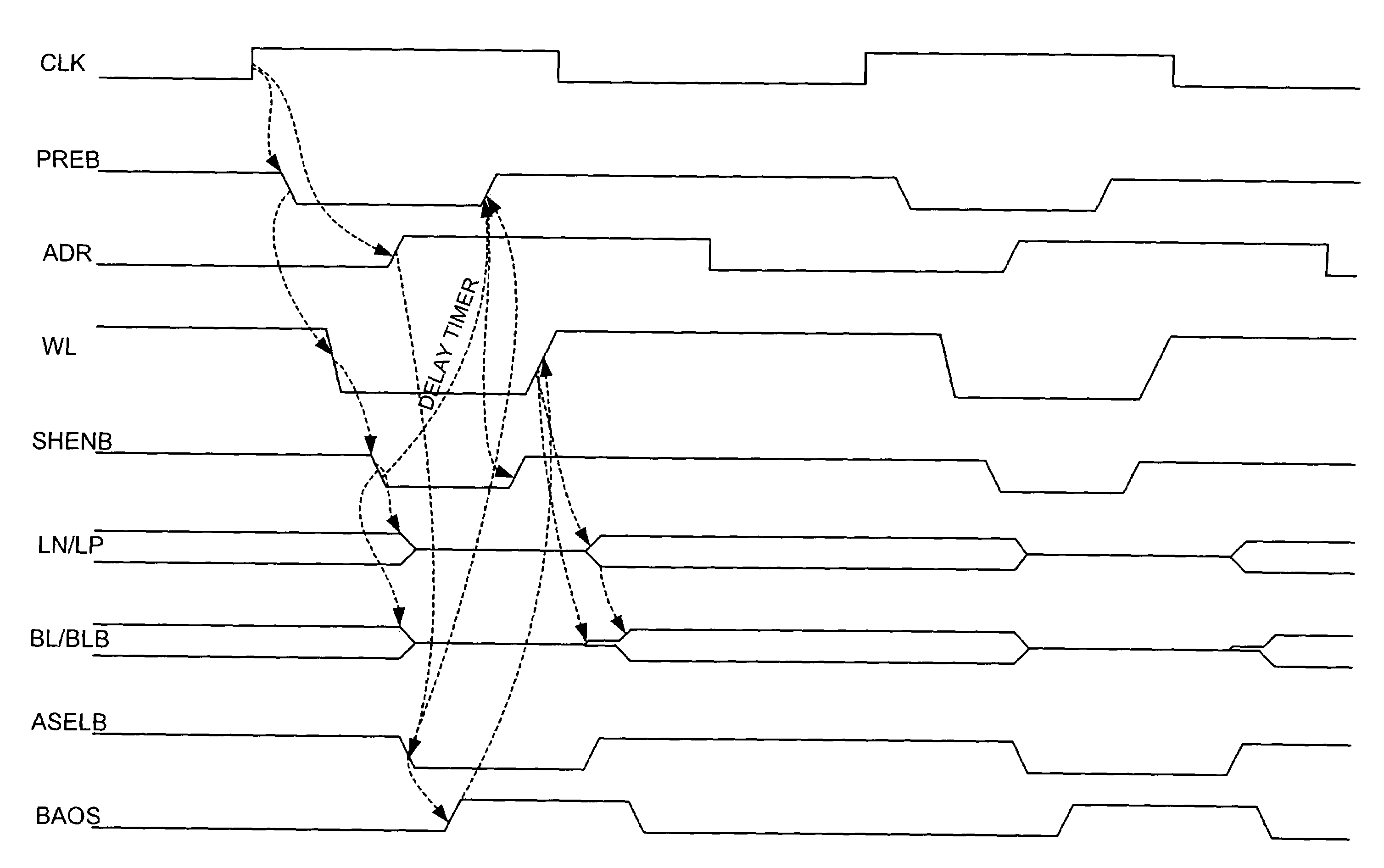
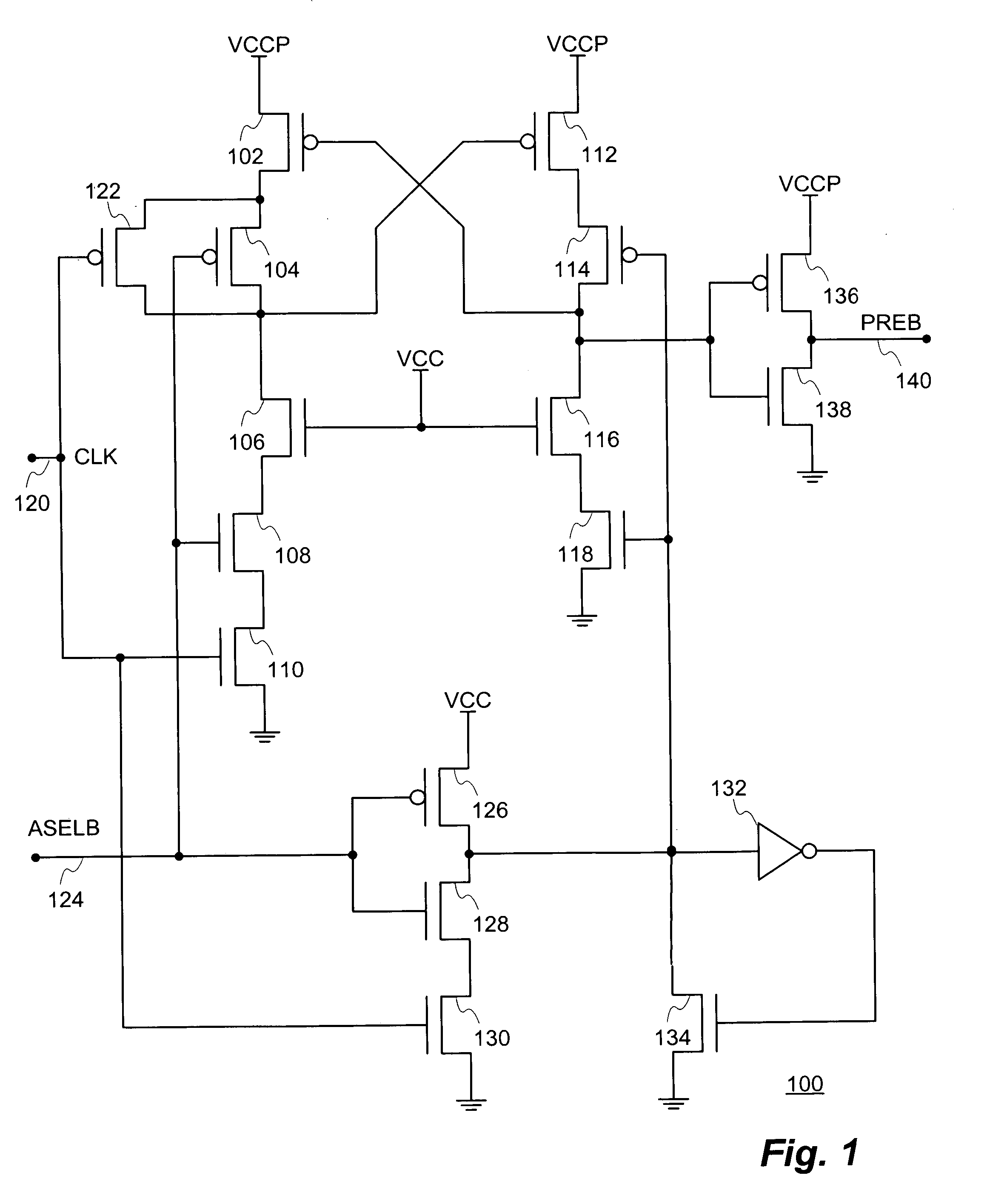
[0016]With reference now to FIG. 1, a schematic diagram of an exemplary main precharge clock (precharge clock 0 bar [POB]) generator 100 is shown for possible use in the implementation of the clock signal initiated precharge technique for active memory subarrays of the present invention. The POB generator 100 comprises series connected P-channel transistors 102 and 104 further in series with N-channel transistors 106, 108 and 110 coupled between a boosted supply voltage source (VCCP) and a reference voltage level of circuit ground. Similarly, series connected P-channel transistors 112 and 114 are connected in series with N-channel transistors 116 and 118 between VCCP and circuit ground.

[0017]An input clock (CLK) signal on line 120 is applied to the gate terminal of P-channel transistor 122, which is connected in parallel with transistor 104, as well as to the gate terminal of transistor 110. An array select bar (ASELB) signal is supplied on line 124 which is coupled to the common co...


PUM


Abstract

A precharge initiated dynamic random access memory (DRAM) technique of especial utility with respect to DRAM devices and other integrated circuit devices incorporating embedded DRAM in which the rising edge of each clock initiates a precharge to those subarrays that were active as opposed to conventional techniques wherein the subarrays are typically precharged so that they are made ready on the rising edge of the clock, which would then start an active cycle. The longer restore time that is achieved can be used to enable the establishment of better logic “1” and “0” levels in the memory cells, to reduce the device clock period and / or to enable other functions to be performed in parallel with the precharge function.

Description

BACKGROUND OF THE INVENTION[0001]The present invention relates, in general, to the field of integrated circuit memory devices and devices incorporating embedded memory arrays. More particularly, the present invention relates to a clock signal initiated precharge technique for active memory subarrays in dynamic random access memory (DRAM) devices and other integrated circuit devices incorporating embedded DRAM.[0002]It has long been a goal of memory design to increase the performance of DRAM in order to support higher speed processors. One method of increasing DRAM performance is to increase the “read” and “write” data rate across the memory bus. SDRAM access times and burst data rates are constantly improving by manufacturing process “shrinks” and improved interconnect technology. Additionally, improved command bus utilization has been achieved by reducing the number of instructions needed to perform certain memory operations. In general, the fewer command cycles which are required ...

Claims


Application Information

Patent Timeline
Patent Type & Authority Patents(United States)
IPC IPC(8): G11C7/00G11C8/00
CPCG11C11/4076G11C11/4087G11C11/4094
Inventor PARRIS, MICHAEL C.HARDEE, KIM C.
Owner SONY CORP
Why Eureka
Try Eureka