Semiconductor device and method for manufacturing same

a technology of semiconductor devices and semiconductors, applied in the direction of semiconductor devices, basic electric elements, electrical equipment, etc., can solve the problems of low controllability of threshold voltage and the inability to manufacture nmosfets having the specified threshold voltage, and achieve the effect of accurate control of threshold voltag

Inactive Publication Date: 2007-01-02
RENESAS ELECTRONICS CORP
View PDF17 Cites 2 Cited by
  • Summary
  • Abstract
  • Description
  • Claims
  • Application Information

AI Technical Summary

Benefits of technology

[0014]In view of the foregoing, an object of the present invention is to provide a semiconductor device having a configuration which allows an accurate control of the threshold voltage by suppressing a reverse short channel effect of an NMOSFET.
[0016]In accordance with the first aspect of the present invention, the semiconductor device including the NMOSFET having a suppressed reverse short channel effect and reduced p-n junction leakage current can be realized.
[0019]In accordance with the second aspect of the present invention, since the source / drain region having the shallower junction and the buffer regions are formed in the NMOSFET region by the two successive ion implantations, the present invention achieves a simple process for fabricating a semiconductor device including an NMOSFET having a suppressed reverse short channel effect and reduced p-n junction leakage current.

Problems solved by technology

In the conventional method for forming the source / drain region of the NMOSFET, a reverse short channel effect of the NMOSFET is noticeable which lowers the controllability of the threshold voltage.
The inability of manufacturing the NMOSFET having the specified threshold voltage is a bar to elevating a production yield of semiconductor devices.

Method used


Image

  • Semiconductor device and method for manufacturing same
  • Semiconductor device and method for manufacturing same
  • Semiconductor device and method for manufacturing same

Examples


Embodiment Construction

[0031]Before describing preferred embodiments of the present invention, the principle of the present invention is described for a better understanding.

[0032]The present inventor has examined a reason of occurrence of the reverse short channel effect to find out the following.

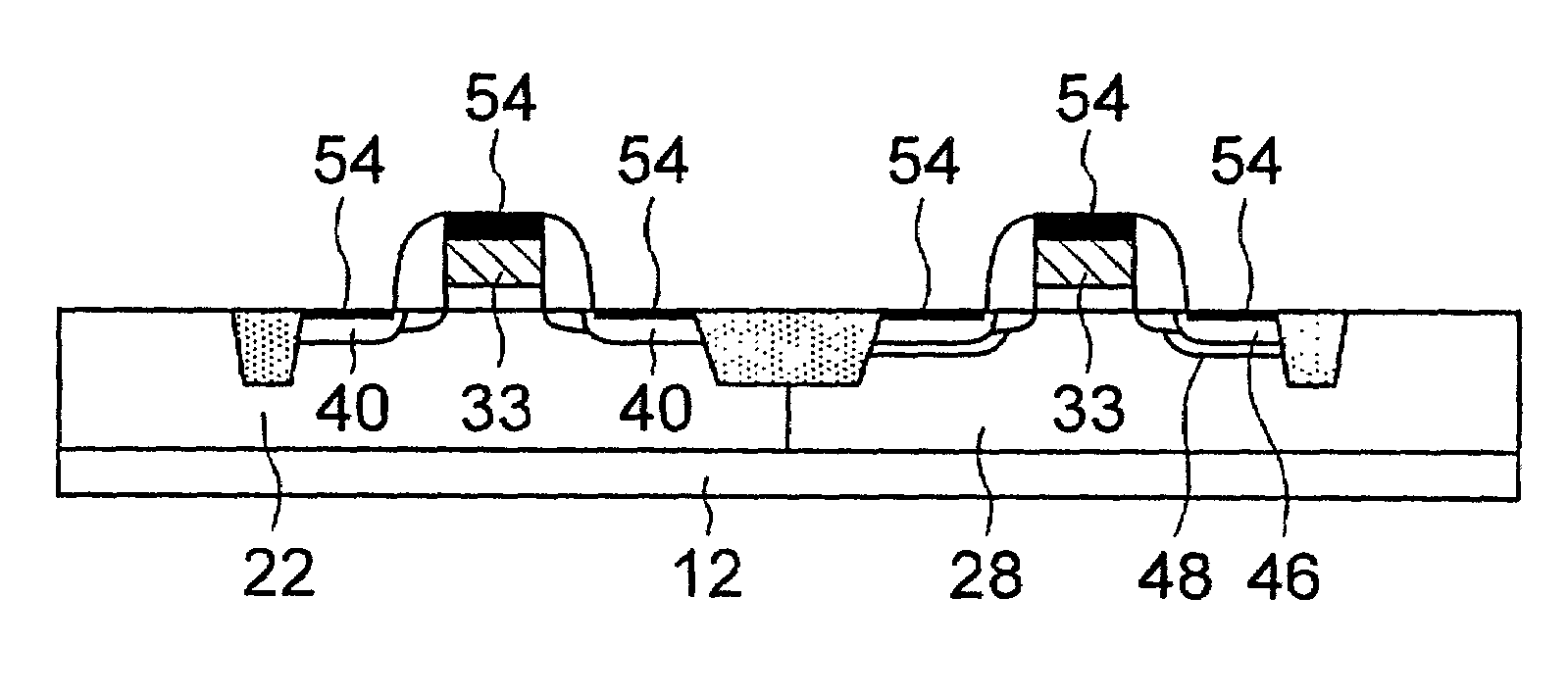
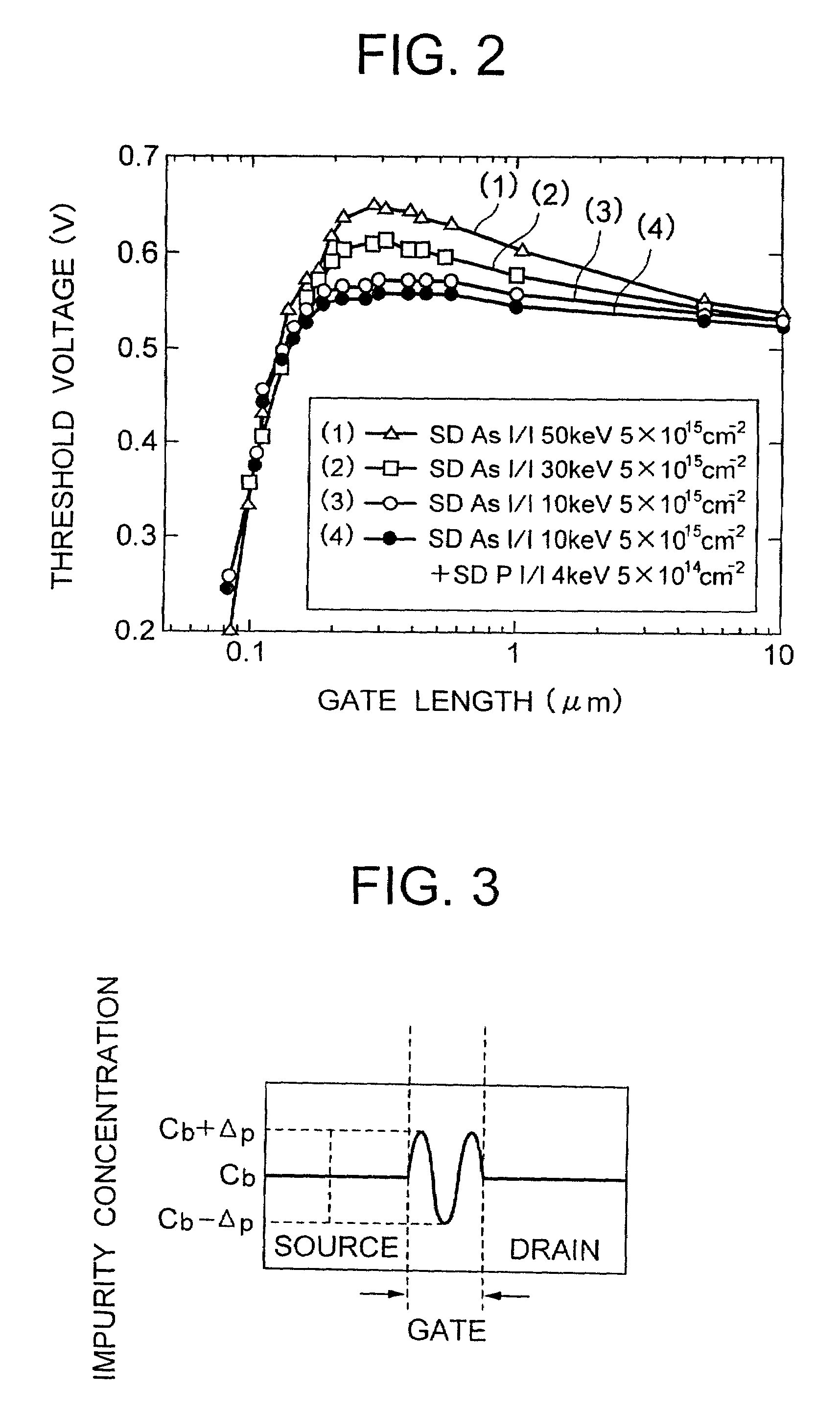
[0033]Point defects are generated in the periphery of an arsenic implanted region at a time of implanting the arsenic ions. As a result, when the arsenic ions are heat-treated for activation, p-type impurities, boron (B), already implanted for forming a channel region causes a transient enhancement diffusion (TED) towards the circumferences of the channel regions due to the above point defects. Accordingly, impurity concentrations are distributed as shown in FIG. 3 so that the concentrations at the both ends of the channel region are high and that at the central part is low.

[0034]Therefore, the low threshold voltage at the central part having the low impurity concentration and the high threshold voltage at the b...


PUM


Abstract

A semiconductor device including an NMOSFET which has an n-type source / drain main region containing arsenic and an n-type source / drain buffer region having arsenic and phosphorous of which a concentration is lower than that of the source / drain main region, and the concentration of the phosphorous in the source / drain buffer region is smaller than the concentration of the arsenic therein. The semiconductor device has a suppressed reverse short channel effect and reduced p-n junction leakage current. Further, the semiconductor device has a larger margin to a certain gate length and a specified threshold voltage to elevate a production yield.

Description

BACKGROUND OF THE INVENTION[0001](a) Field of the Invention[0002]The present invention relates to a semiconductor device including an NMOSFET and a method for manufacturing the same, more in detail, to the semiconductor device including the NMOSFET having an accurate threshold voltage at a designed value due to excellent controllability of the threshold voltage, and reduced p-n junction leakage current, and the method for manufacturing the same.[0003](b) Description of the Related Art[0004]A high performance LSI has been realized which includes a CMOSFET including an n-channel MOSFET and a p-channel MOSFET. Reduction of the length of the channels of the MOSFET and the resulting shallower junction of the source / drain region are progressing.[0005]In order to form a shallower source / drain junction in an n-channel MOS transistor, ions having a smaller thermal diffusion coefficient during heat treatment and activation thereof are used as n-type impurities for ion-implantation.[0006]Heret...

Claims


Application Information

Patent Timeline
Patent Type & Authority Patents(United States)
IPC IPC(8): H01L21/336H01L21/8234H01L21/8238H01L21/265H01L29/78H01L21/60
CPCH01L21/26506H01L21/823814H01L21/26513H01L29/665H01L29/78
Inventor IMAI, KIYOTAKA
Owner RENESAS ELECTRONICS CORP
Why Eureka
Try Eureka