Variable capactor structure and method of manufacture
a variable capacitor and capactor technology, applied in the direction of diodes, semiconductor devices, electrical apparatus, etc., can solve the problems of affecting the resistance it is difficult to achieve further improvement in the operating efficiency of the variable capacitor, so as to achieve the effect of small resistan
- Summary
- Abstract
- Description
- Claims
- Application Information
AI Technical Summary
Benefits of technology
Problems solved by technology
Method used
Image
Examples
first embodiment
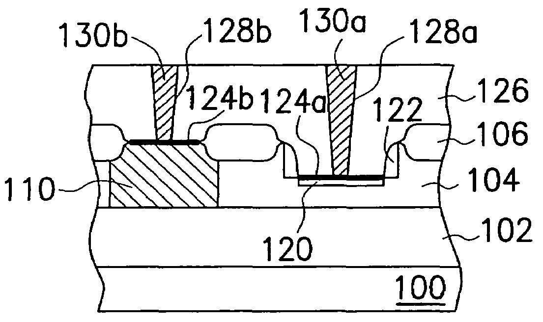
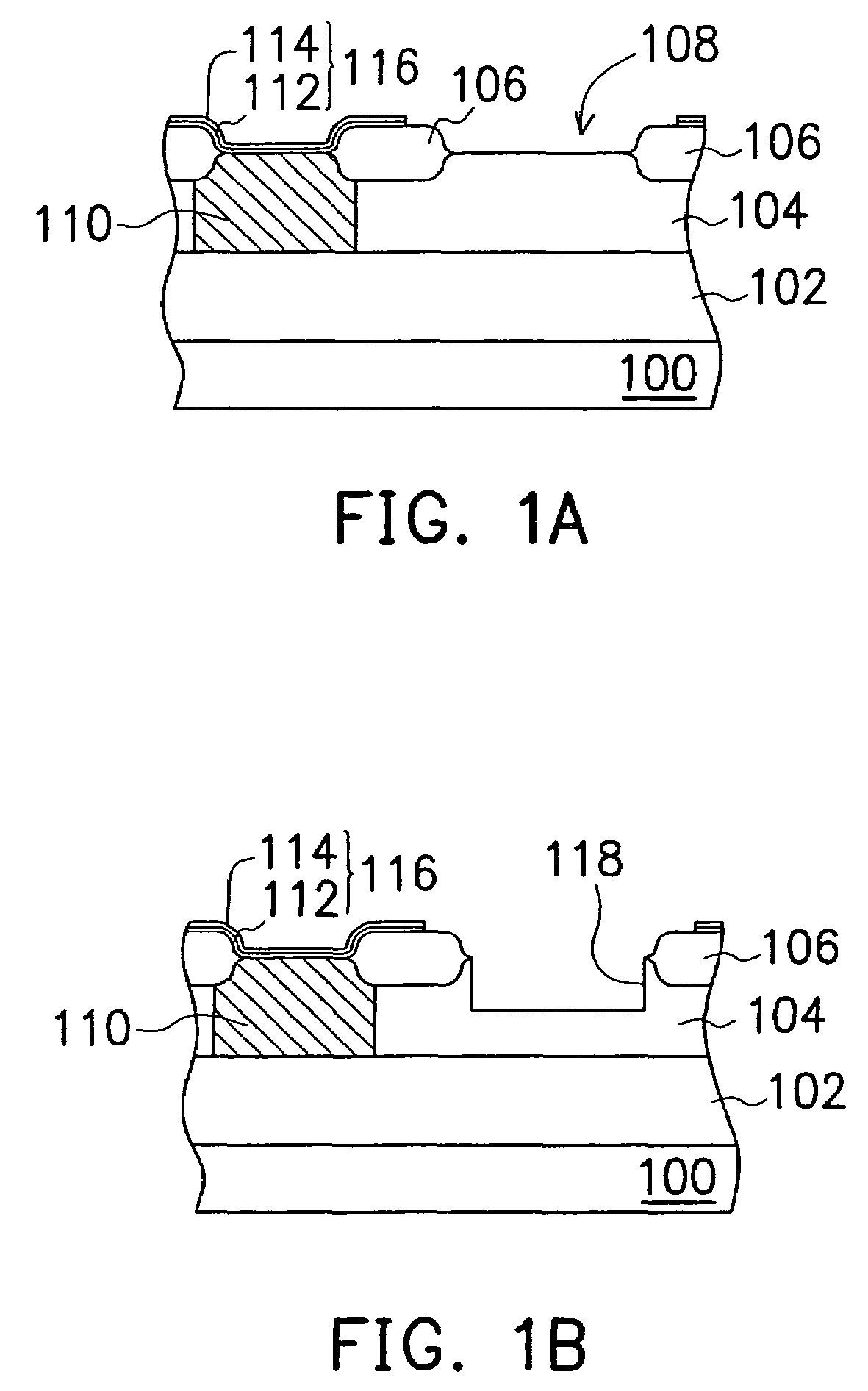
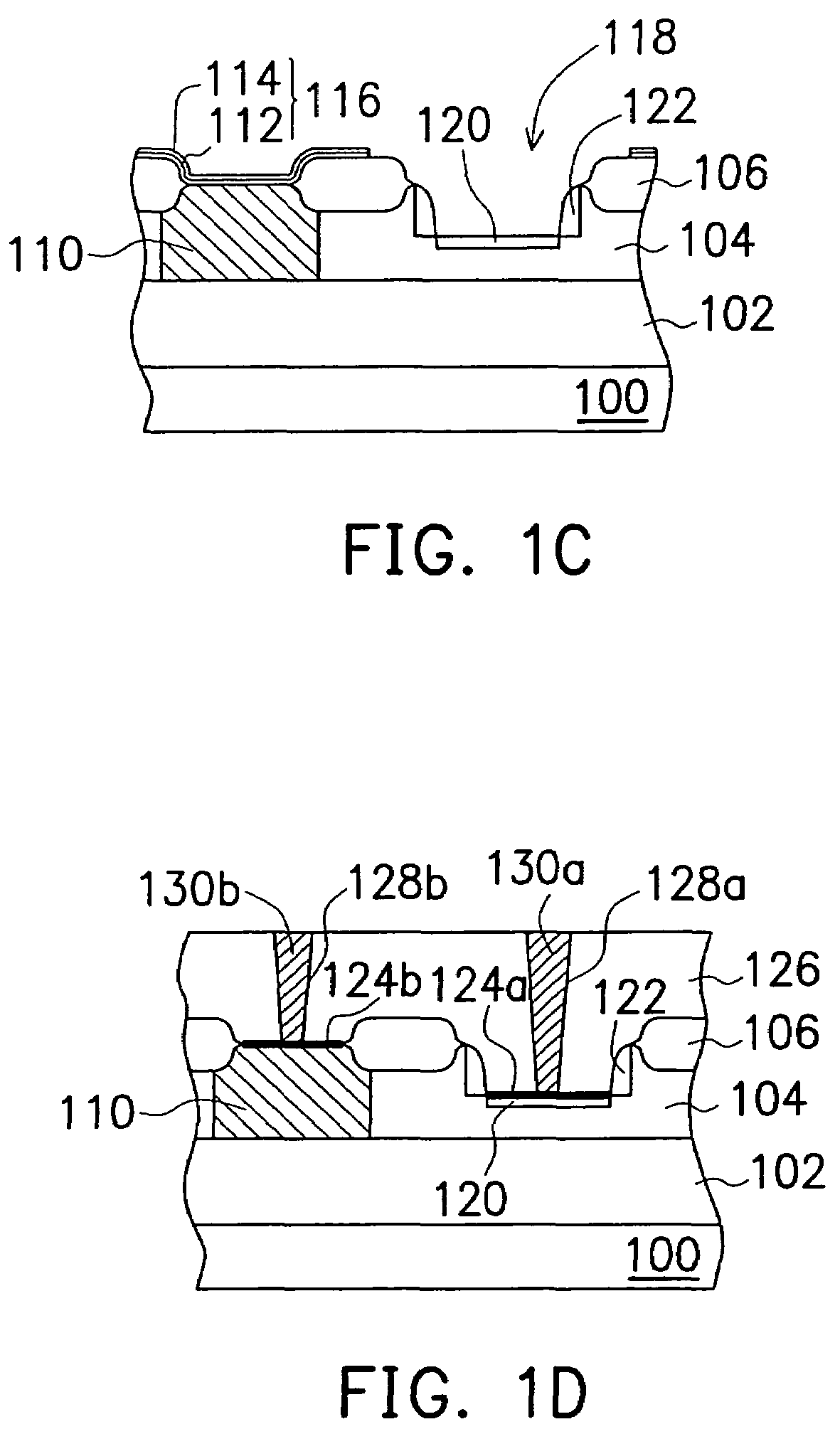
[0037]In the first embodiment, the P+-doped region 120 is formed at the bottom of the opening 118. Hence, the thickness from the P+-doped region 120 to the N+ buried layer 102 is reduced. Ultimately, overall resistance of the variable capacitor decreases considerably.
[0038]In addition, a portion of the fabricating step may combine with the bipolar manufacturing processes. Hence, the total number of masks in manufacturing the variable capacitor in this invention is identical to a conventional process. In other words, the manufacturing process is able to reduce the resistance of a variable capacitor without any increase in the number of required masks.
[0039]Furthermore, the variable capacitor comprises a P+-doped region, a N+ buried layer and a P-type deep collector. However, other arrangements are also possible such as an N+-doped region, a P+ buried layer and an N-type deep collector.
[0040]FIGS. 2A to 2E are schematic cross-sectional views showing the progression of steps for produc...
second embodiment
[0049]In the second embodiment, the P+-doped region 212b is formed in the N-well 204 at the bottom of the opening 208b. Hence, the distance from the P+-doped region 212b to the N+ buried layer 202 is reduced. Ultimately, overall resistance of the variable capacitor decreases considerably.
[0050]Furthermore, a portion of the fabricating step may combine with the bipolar manufacturing processes. Hence, the total number of masks in manufacturing the variable capacitor in this invention is identical to a conventional process. In other words, the manufacturing process is able to reduce the resistance of a variable capacitor without any increase in the number of required masks.
[0051]Although the variable capacitor comprises a P+-doped region and a N+ buried layer, other arrangements are also possible, such as an N+-doped region and a P+ buried layer.
[0052]FIGS. 3A to 3F are schematic cross-sectional views showing the progression of steps for producing a variable capacitor according to a th...
third embodiment
[0061]In the third embodiment, the initial and final points of the variable capacitor are formed in the same active area. Hence, overall layout area of the capacitor is reduced.
[0062]Unlike a conventional variable capacitor that requires a deep collector to connect with the N+ buried layer, the contacts directly contact with the N+ buried layer. Because the contact is made from low resistant metallic material while a conventional deep collector is made from doped silicon, resistivity of the deep collector is considerably higher than the contact. In this invention, the buried layer 302 is connected through the contact 324b. Consequently, resistance of the variable capacitor is further reduced and the quality factor of the variable capacitor is increased.
[0063]In addition, the P+-doped region 312 is formed in the N-well 304 at the bottom of the opening 308. Hence, the distance from the P+-doped region 312 to the N+ buried layer 302 is reduced. Ultimately, overall resistance of the var...
PUM
 Abstract
Description
Claims
Application Information


