Three-dimensional integrated capacitance structure

a capacitance structure and three-dimensional technology, applied in capacitors, semiconductor devices, semiconductor/solid-state device details, etc., can solve the problems of high non-linear capacitors, biases that are incompatible with the low power supply voltage used in modern circuits, and mos capacitors are polarized, so as to achieve high capacitance density

Active Publication Date: 2007-01-09
ANALOG DEVICES INC
View PDF4 Cites 28 Cited by
  • Summary
  • Abstract
  • Description
  • Claims
  • Application Information

AI Technical Summary

Benefits of technology

[0009]A three-dimensional integrated capacitance structure is presented which overcomes the problems noted above, providing relatively high capacitance density without requiring any special processing steps.

Problems solved by technology

Unfortunately, the polysilicon layers and terminals deposited thereon form a MOS structure.
This leads to a highly non-linear capacitor unless a large DC bias is maintained across the capacitor.
Such biases are incompatible with the low power supply voltages used with modern circuits.
Further, MOS capacitors are polarized, and therefore cannot be used in circuits such as switched-capacitor circuits in which the terminals of the capacitor are flipped in polarity.
While such capacitors avoid the problems discussed above with respect to MOS capacitors, metal—metal capacitors have two drawbacks of their own.
Second, such capacitors suffer from parasitic, or “back-plate” capacitance between one, or both, of the terminals and the substrate of the IC.
However, special processing steps are typically required to implement these devices.

Method used


Image

  • Three-dimensional integrated capacitance structure
  • Three-dimensional integrated capacitance structure
  • Three-dimensional integrated capacitance structure

Examples


Embodiment Construction

[0022]The present invention is a three-dimensional integrated capacitance structure which provides a relatively high capacitance density, and can be fabricated using standard process sequences. The structure is particular suitable for use on ICs fabricated with processes having no specialized capacitor structure.

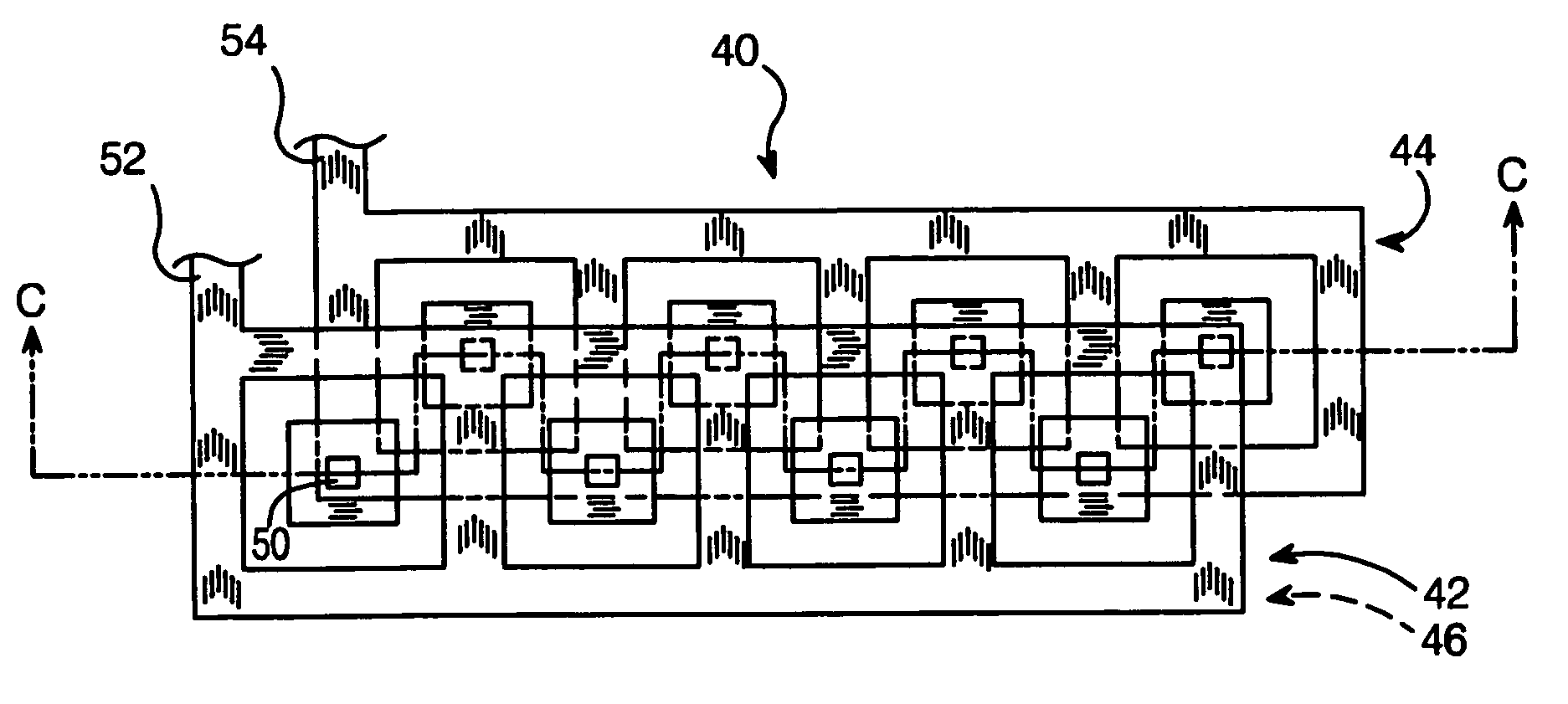
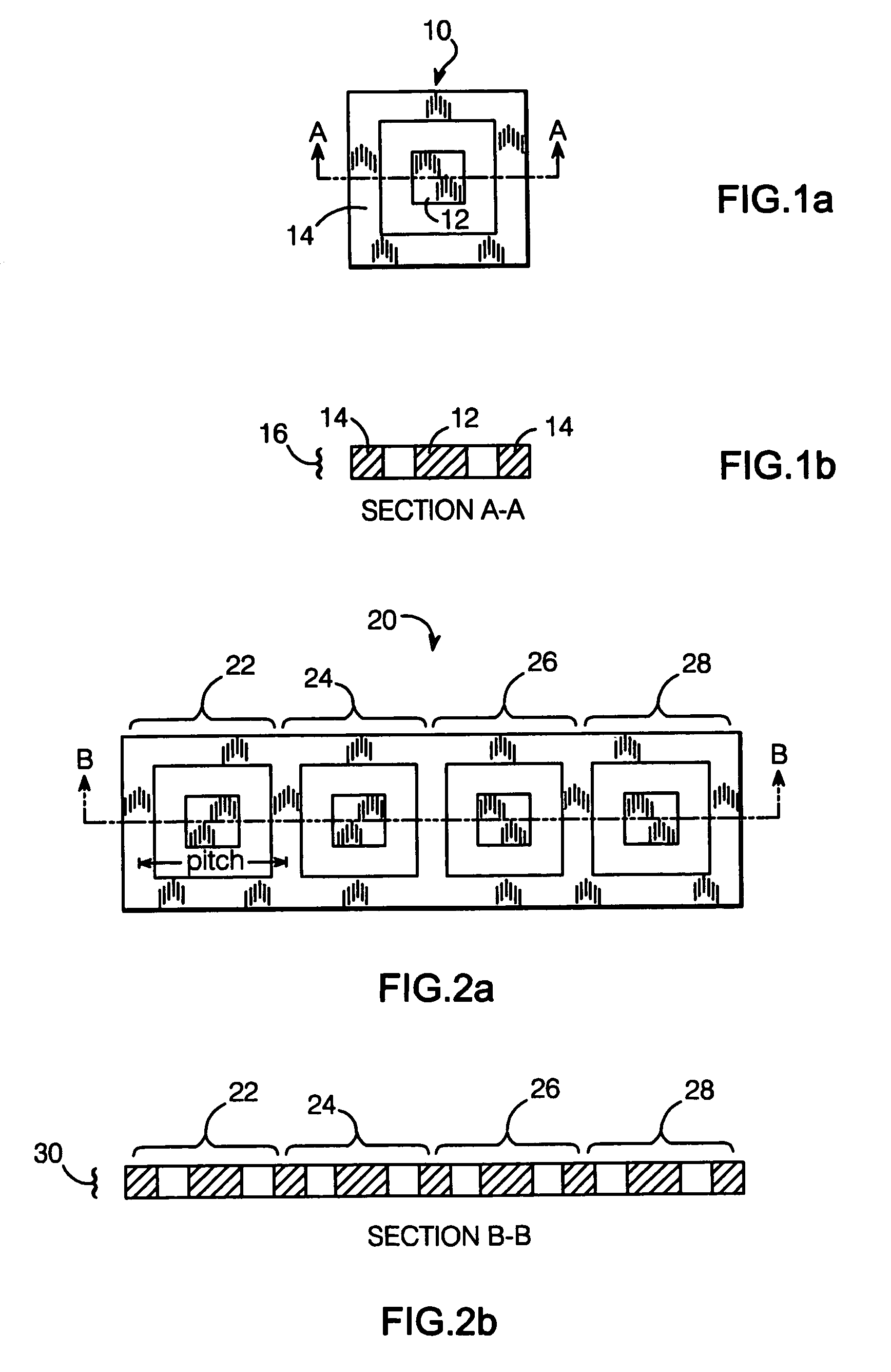
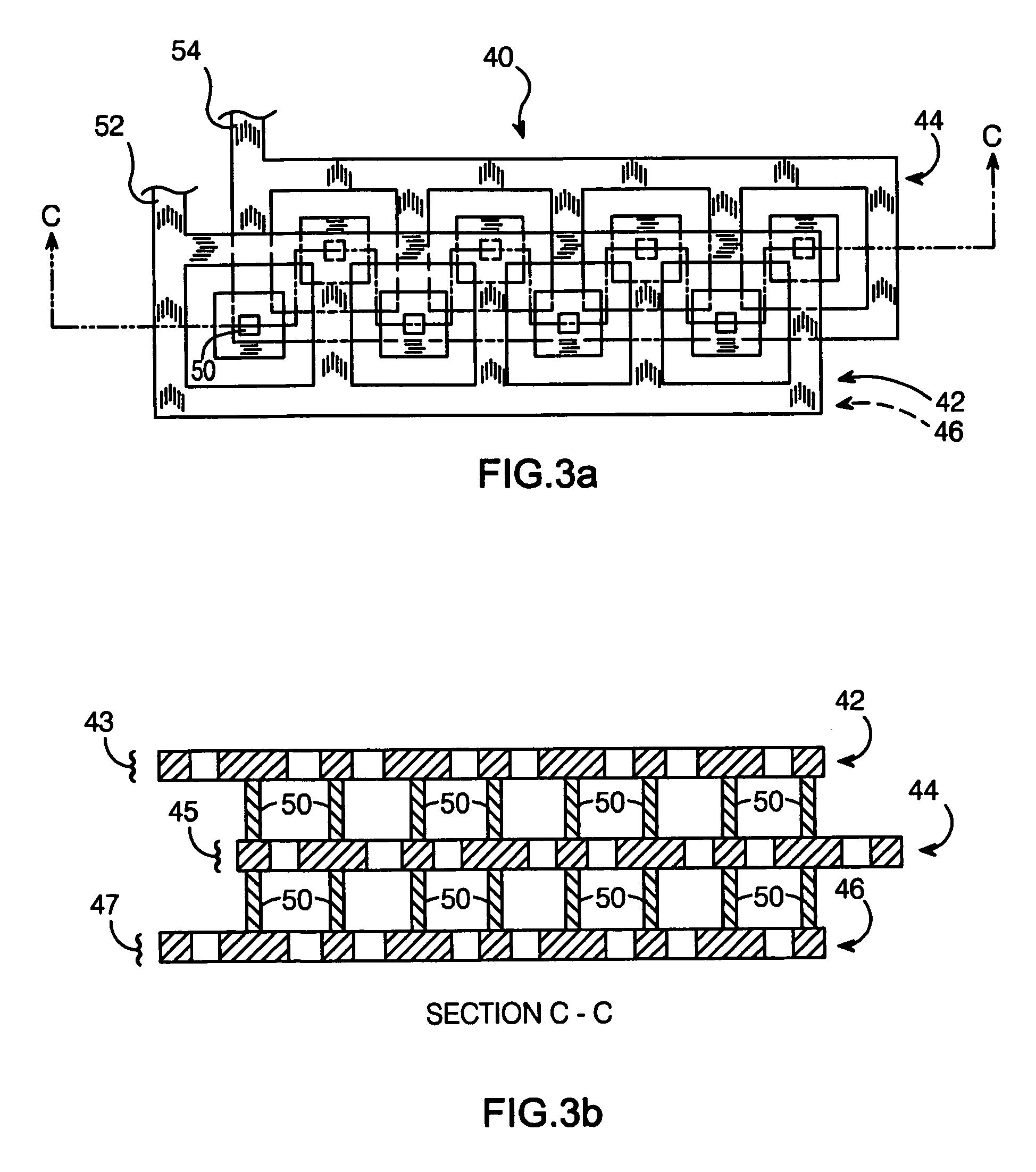
[0023]The capacitance structure is created with layers of arrayed unit cells. A plan view of a typical unit cell is shown in FIG. 1a, with a corresponding cross-sectional view cut along section line A—A shown in FIG. 1b. Each unit cell 10 comprises a center conductor 12, and a conducting ring 14 which surrounds the center conductor. The capacitance structure is formed as part of an IC; center conductor 12 and conducting ring 14 are fabricated on the same layer 16 of the IC.

[0024]Unit cells are assembled into an array, which comprises a plurality of unit cells tiled on a given IC layer at a predetermined pitch. A plan view of such an array 20 is shown in FIG. 2a, with a corre...


PUM


Abstract

A three-dimensional integrated capacitance structure comprises at least two arrays of “unit cells” on respective layers of an IC, with each unit cell comprising a center conductor and a conducting ring which surrounds the center conductor. Each array comprises a plurality of unit cells, tiled on a given IC layer at a predetermined pitch. The arrays are arranged vertically such that adjacent vertical arrays are offset in the x and y dimensions by a predetermined fraction—preferably ½—of the unit cells' pitch. The structure includes vias arranged to interconnect the arrays such that each center conductor is connected to a conducting ring of the array immediately above and/or below the center conductor, and such that each conducting ring is connected to a center conductor of the array immediately above and/or below the conducting ring.

Description

BACKGROUND OF THE INVENTION[0001]1. Field of the Invention[0002]This invention relates to the field of integrated capacitors.[0003]2. Description of the Related Art[0004]Integrated circuits (ICs), particularly those which implement analog circuitry, often have a need for a capacitance element. Such capacitances provide many different circuit functions, such as filtering and compensation.[0005]Traditional analog IC processes construct capacitors by sandwiching a dielectric layer between conductors. For example, a polysilicon layer deposited over a silicon substrate can serve as a capacitor's plates, with an oxide layer between the plates serving as a dielectric layer. Oxide layers are very thin, and hence this type of structure has a very high specific capacitance. Unfortunately, the polysilicon layers and terminals deposited thereon form a MOS structure. This leads to a highly non-linear capacitor unless a large DC bias is maintained across the capacitor. Such biases are incompatibl...

Claims


Application Information

Patent Timeline
Patent Type & Authority Patents(United States)
IPC IPC(8): H01L29/00
CPCH01L23/5223H01L28/92H01L2924/0002H01L2924/00
Inventor PETTIT, RICKY L.
Owner ANALOG DEVICES INC
Why Eureka
Try Eureka