Photoelectric conversion apparatus, manufacturing method therefor, and X-ray imaging apparatus

Inactive Publication Date: 2007-01-16
CANON KK
View PDF5 Cites 11 Cited by
  • Summary
  • Abstract
  • Description
  • Claims
  • Application Information

AI Technical Summary

Benefits of technology

[0021]The present invention has been made in consideration of the above problems, and has as its object to easily and reliably perform proper exposure control in executing radiography.

Problems solved by technology

A phototimer, however, roughly has two problems: one based on the sensitivity difference between a means for obtaining an X-ray image and the phototimer, and the other based on the number of phototimers to be installed.
It is, however, difficult to precisely match the sensitivity characteristics (tube voltage characteristics and linearity), signal-to-noise ratio (S / N ratio), and offset amount of the phototimer with those of the X-ray imaging apparatus.
Consequently, accurate exposure precision cannot be obtained.
In consideration of installation places and cost, it is not realistic to install phototimers at positions corresponding to various regions.
Even in this case, since there are physical differences between adults and children, and different densities are required depending on diagnostic regions, exposure control cannot always be relied on the phototimers.
Owing to the above problems, according to the conventional techniques, even if an X-ray imaging apparatus is equipped with phototimers, radiography cannot be relied on the phototimers in all radiographic conditions.
In order to reduce failures in radiography, therefore, a patient is irradiated with a relatively high dose of X-rays to increase the contrast, resulting in an increase in the radiation dose of the patient.
At an early stage of proliferation of digital X-ray imaging apparatuses on the market, only a small amount of clinical data has been obtained, leading to poor exposure precision.
These problems have interfered with the development and widespread use of X-ray imaging apparatuses.

Method used


Image

  • Photoelectric conversion apparatus, manufacturing method therefor, and X-ray imaging apparatus
  • Photoelectric conversion apparatus, manufacturing method therefor, and X-ray imaging apparatus
  • Photoelectric conversion apparatus, manufacturing method therefor, and X-ray imaging apparatus

Examples


first embodiment

(First Embodiment)

[0044]The first embodiment of the present invention will be described.

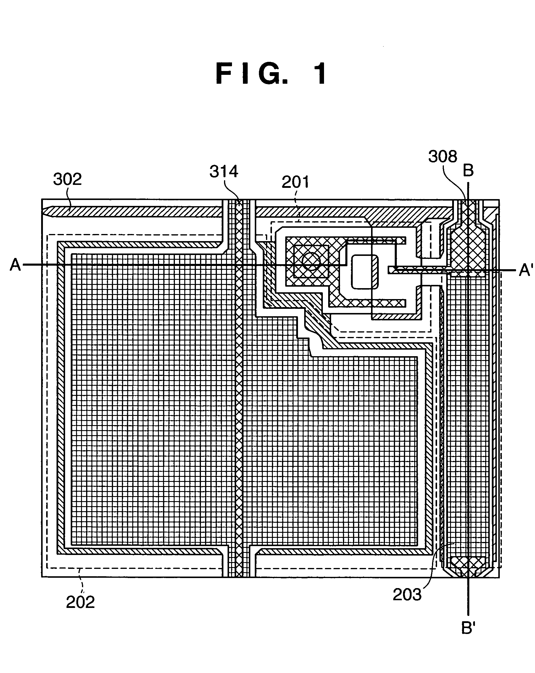
[0045]FIG. 1 is a view showing an example of one pixel of the two-dimensional sensor used in a digital X-ray imaging apparatus according to the first embodiment of the present invention. For the sake of convenience, FIG. 1 shows no phosphor or the like.

[0046]Each pixel of the two-dimensional sensor has a MIS (Metal-Insulator-Semiconductor) type photoelectric conversion unit 202 placed as a photoelectric conversion element which converts visible light emitted from a phosphor into an electrical signal and stores it, and a TFT (Thin-Film-Transistor) 201 placed as a transfer device for transferring the electric charge stored in the MIS type photoelectric conversion unit 202.

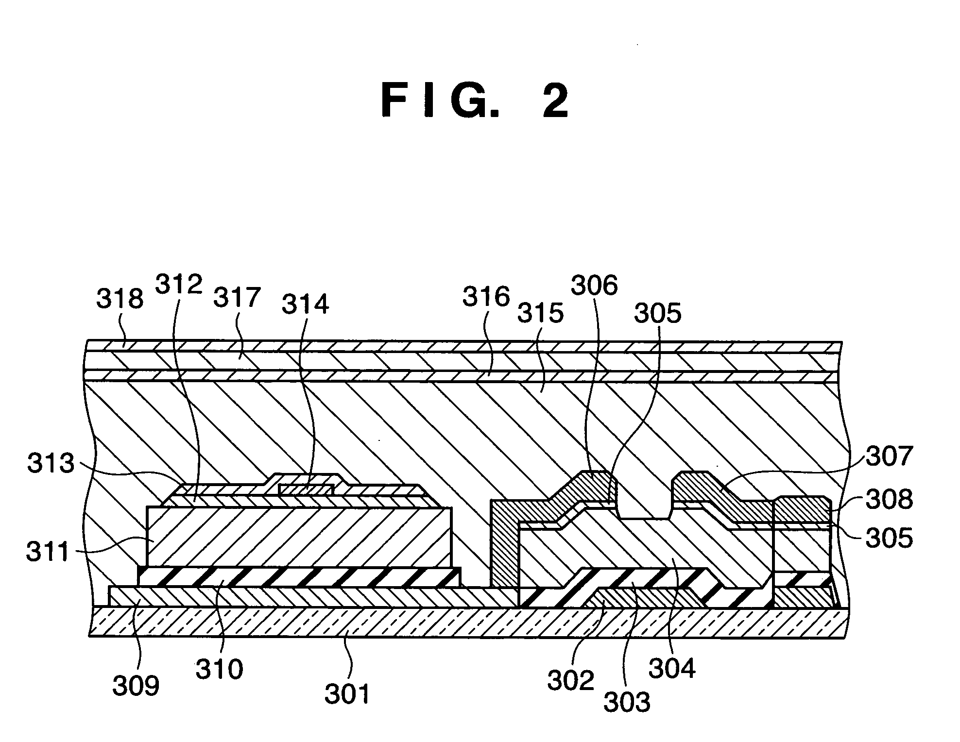
[0047]A gate electrode 302, sensor bias line 314, and signal line 308 are connected to the above pixel. The gate electrode 302 drives the TFT 201. The sensor bias line 314 applies a voltage required for photoelectric conversion or...

second embodiment

(Second Embodiment)

[0116]The second embodiment of the present invention will be described next. This embodiment mainly differs from the first embodiment in the arrangement of a two-dimensional sensor. The same reference numerals as in FIGS. 1 to 8 in the first embodiment denote the same parts in the second embodiment, and hence a detailed description thereof will be omitted.

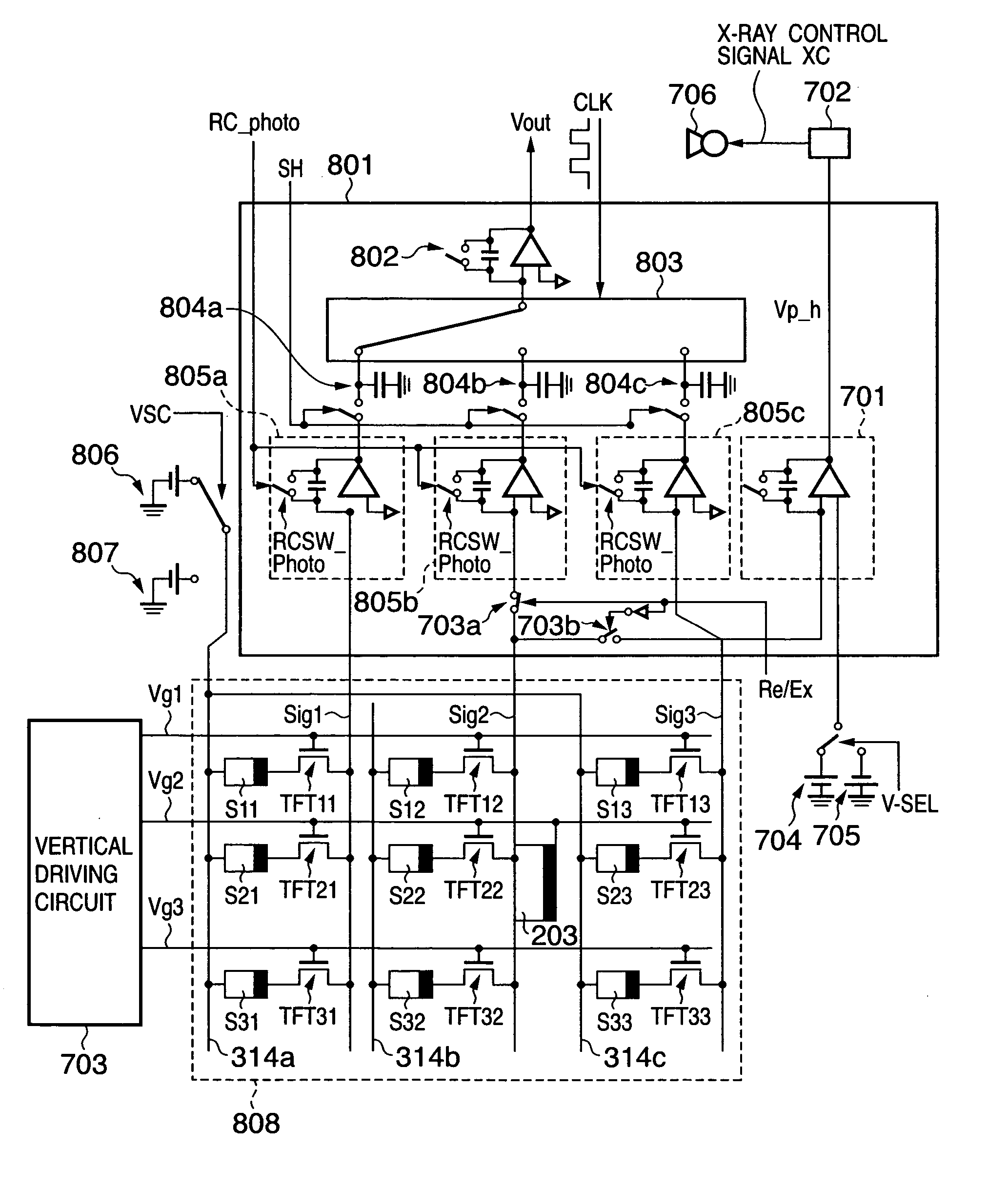
[0117]FIG. 9 shows the schematic arrangement of a photoelectric conversion apparatus according to this embodiment. More specifically, FIG. 9 shows the photoelectric conversion apparatus in which pluralities of signal amplification circuits and vertical driving circuits are connected to a sensor substrate on which 2,500×2,500 pixels are arranged.

[0118]A total of 20 signal amplification circuits 801 shown in FIG. 7 are connected to the sensor substrate, 10 circuits each on the upper and lower sides in FIG. 9. One signal amplification circuit 801 is connected to 250 signal lines Sig. As shown in FIG. 9, phototimer d...

third embodiment

(Third Embodiment)

[0129]The third embodiment of the present invention will be described next. Note that the first and third embodiments differ in the detailed arrangement of a photoelectric conversion element. More specifically, the first embodiment uses a MIS type photoelectric conversion unit as a photoelectric conversion element, whereas the third embodiment uses a PIN type photoelectric conversion unit as a photoelectric conversion element. The same reference numerals as in FIGS. 1 to 8 in the first embodiment denote the same parts in the third embodiment, and hence a detailed description thereof will be omitted.

[0130]FIG. 10 is a sectional view of a pixel formed from a combination of a PIN type photoelectric conversion unit as a photoelectric conversion element and a TFT as a transfer device.

[0131]Like the TFT 201 in the first embodiment described above, the TFT is constituted by a gate electrode 1102 made of chromium, aluminum, or an aluminum alloy and formed on a glass substr...


PUM


Abstract

In an X-ray imaging apparatus, an optical sensor (phototimer detection unit) corresponding to a conventional photomultiplier is incorporated in a two-dimensional sensor (on a signal line), and a signal from the phototimer detection unit is integrated and monitored, thereby performing exposure control. This makes it possible to incorporate the phototimer detection unit without affecting the aperture ratio of pixels which influence the performance of the X-ray imaging apparatus and the characteristics of a MIS type photoelectric conversion unit, thereby performing proper exposure control.

Description

FIELD OF THE INVENTION[0001]The present invention relates to a photoelectric conversion apparatus, a manufacturing method thereof, and an X-ray imaging apparatus and, more particularly, to a photoelectric conversion apparatus, a manufacturing method therefor, and an X-ray imaging apparatus which are suitable for exposure control.BACKGROUND OF THE INVENTION[0002]In X-ray radiography, an automatic exposure control device (phototimer) is widely used. The phototimer is placed behind or in front of a film to convert X-rays transmitted through an object to be radiographed into an electrical signal, and shuts off X-rays when the integral of this electrical signal reaches a predetermined value, thereby keeping the density of an X-ray image constant.[0003]FIG. 13 shows the arrangement of a conventional phototimer.[0004]As shown in FIG. 13, the phototimer is constituted by a phosphor 108 and photomultiplier 112. The phototimer converts X-rays 102 transmitted through a human body 103 into ligh...

Claims


Application Information

Patent Timeline
IPC IPC(8): H01L31/00H01L25/00H01L27/00H05G1/70H01L27/146A61B6/00G01T1/24G01T1/29H01L27/14H01L31/10H04N5/32H04N5/369H04N5/374
CPCG01T1/2928H01L27/14603H01L27/14609H04N5/32H04N5/353H01L27/14658H04N5/3696H04N25/53H04N25/702H04N25/70
Inventor YAGI, TOMOYUKI
Owner CANON KK
Why Eureka
Try Eureka