Optical transceiver

Inactive Publication Date: 2007-01-23
NEC CORP
View PDF7 Cites 4 Cited by
  • Summary
  • Abstract
  • Description
  • Claims
  • Application Information

AI Technical Summary

Benefits of technology

[0020]Accordingly, an object of the present invention is to provide an optical transceiver having a transmitter section and a receiver section formed on a substrate to be close to each other, which suppresses effectively the electrical and optical crosstalk between the transmitter section and the receiver section.
[0021]Another object of the present invention is to provide an optical transceiver having a transmitter section and a receiver section formed on a substrate to be close to each other, in which electromagnetic wave and light generated in the transmitter section are effectively prevented from affecting the receiver section.
[0022]Still another object of the present invention is to provide an optical transceiver having a transmitter section and a receiver section formed on a substrate to be close to each other, which is easily fabricated at high mass-productivity.
[0038]With the optical transceiver according to the invention, the conductive first connection member that allows the first and second light beams to respectively penetrate the same through the first and second openings is fixed near the substrate. Therefore, the electromagnetic wave emitted from the light-emitting element in the transmitter section and the extrinsic electromagnetic noise are prevented from affecting the receiver section.
[0040]Moreover, the conductive first connection member has the first and second openings that allow the first and second light beams to penetrate the same, respectively. Therefore, the amount of stray light entering the receiver section is decreased. This means that optical crosstalk between the transmitter and receiver sections is suppressed.
[0042]Accordingly, the accuracy or precision for the diameter and pitch of the first and second openings of the first connection member is not so strict as the ferrule used in the prior-art transceiver of FIG. 1. As a result, the conductive first connection member can be easily produced and the obtainable mass-productivity is raised or improved.

Problems solved by technology

However, the above-described prior-art optical transceiver with reference to FIG. 1 has the following problems.
In this case, however, another problem will occur.
However, such a precise hole-formation processing to a metal piece is very difficult to be realized.
Furthermore, the obtainable productivity for this hole-formation processing will be low and thus, it will not be acceptable.
In this case also, however, another problem will occur.

Method used


Image

  • Optical transceiver
  • Optical transceiver
  • Optical transceiver

Examples


first embodiment

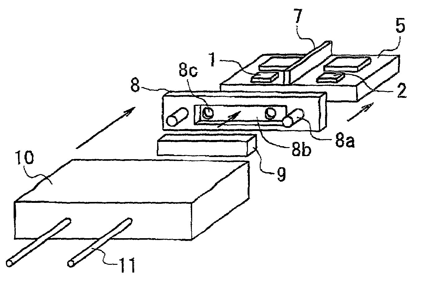
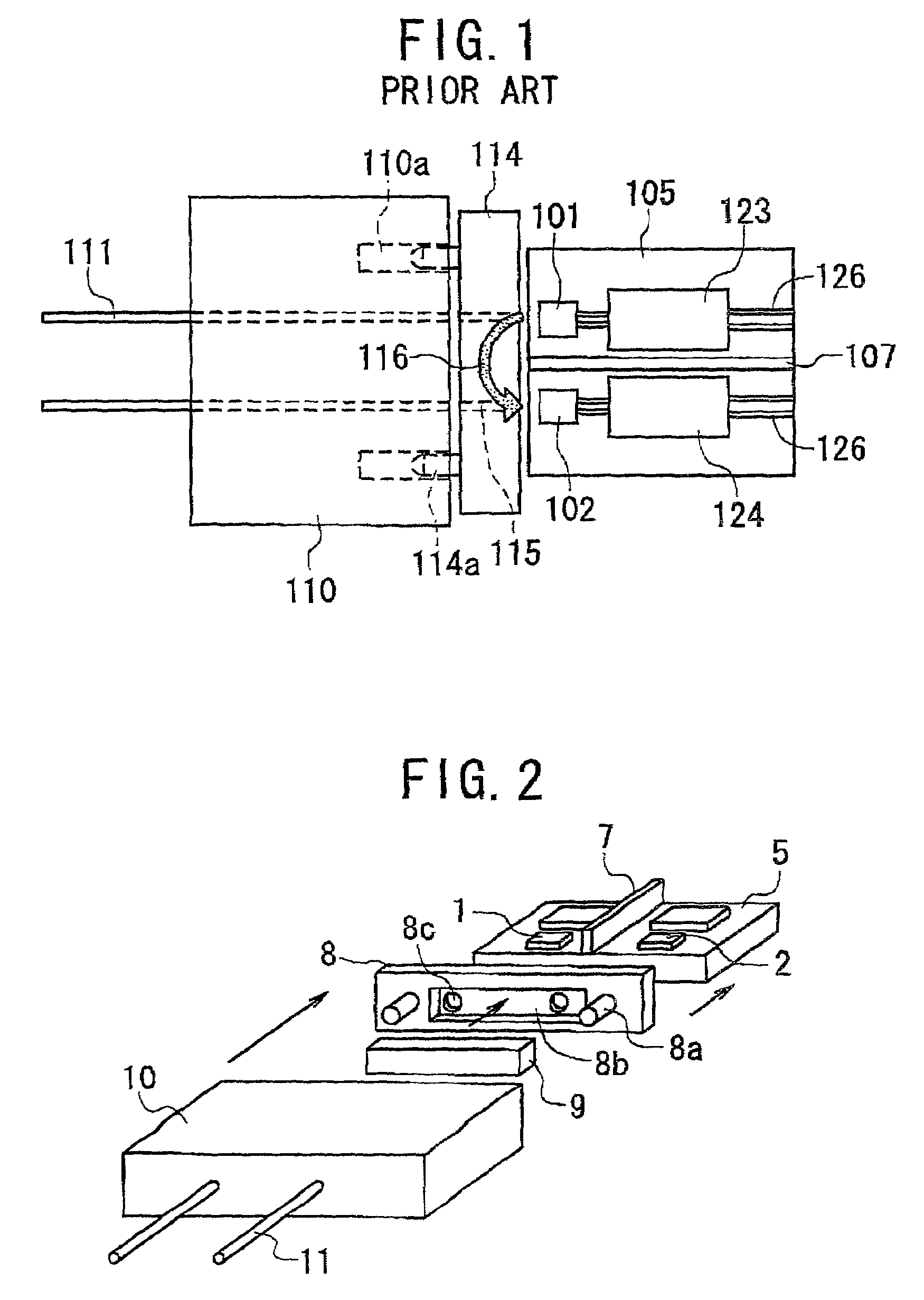
[0056]An optical transceiver according to a first embodiment of the invention is shown in FIGS. 1 and 2.

[0057]As shown in FIGS. 1 and 2, the transceiver of the first embodiment comprises a rectangular substrate 5, a transmitter section formed on the surface of the substrate 5, and a receiver section formed on the surface of the substrate 5 to be close to the transmitter section. Signal lines 6, power supply lines (not shown), and ground lines (not shown) are formed on the surface of the substrate 5. The signal lines 6 are used for transferring electrical signals to be sent to or from the transmitter section and for transferring electrical signals to be sent to or from the receiver section. The power supply lines are used for supplying a specific power supply voltage to the transmitter and receiver sections. The ground lines are used for electrically grounding the transmitter and receiver sections.

[0058]The transmitter section includes a light-emitting element 1 (e.g., a laser diode)...

second embodiment

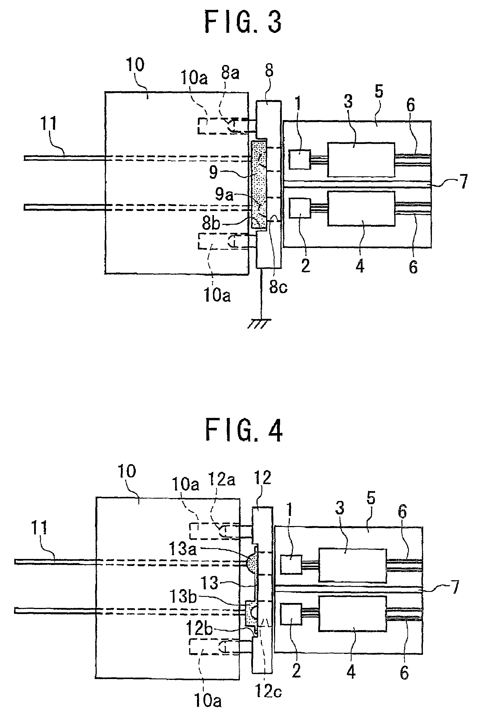
[0086]FIGS. 4 and 5 show the configuration of an optical transceiver according to a second embodiment of the invention. This transceiver has the same configuration as the transceiver of the first embodiment of FIGS. 1 and 2, except that a plate-shaped metal-covered glass member 12 is used instead of the plate-shaped metallic member 8, and that a micro-lens pair 13 with a convex micro-lens 13a and a concave micro-lens 13b is used instead of the plate-shaped transparent member 9.

[0087]As shown in FIG. 5, the plate-shaped transparent glass member 12 is formed by a glass plate 12d to which a light-absorbing additive is added, and a plated metal film 12e covering the whole surface of the plate 12d. On the flat front face of the member 12, a rectangular recess 12b is formed in such a way as to receive the micro-lens pair 13. The recess 12b is substantially the same as the recess 8b of the member 8 in the first embodiment. The micro-lens pair 13 is fittingly inserted into the recess 12b an...


PUM


Abstract

An optical transceiver having a transmitter section and a receiver section formed on a substrate to be close to each other is provided, which suppresses the electrical and optical crosstalk between the transmitter section and the receiver section. The transceiver comprises: (a) a substrate; (b) a transmitter section formed on the substrate and including a light-emitting element; (c) a receiver section formed on the substrate to be close to the transmitter section and including a light-receiving element; (d) a conductive first connection member fixed near the substrate; and (e) a transparent second connection member fixed near the first member in such a way as to block the first opening and the second opening of the first member from a front of the first member. The first member has a first opening that allows a first light beam to penetrate the first member and a second opening that allows a second light beam to penetrate the first member. The first opening is aligned to an optical axis of the light-emitting element. The second opening is aligned to an optical axis of the light-receiving element.

Description

BACKGROUND OF THE INVENTION[0001]1. Field of the Invention[0002]The present invention relates to an optical transceiver. more particularly, the invention relates to an optical transceiver having a transmitter section and a receiver section formed on a substrate to be close to each other, which suppresses the electrical and optical crosstalk between the transmitter section and the receiver section.[0003]2. Description of the Related Art[0004]FIG. 1 schematically shows the configuration of a prior-art optical transceiver of this type.[0005]As shown in FIG. 1, the transceiver comprises a substrate 105, a transmitter section and a receiver section mounted on the surface of the substrate 105, and a ferrule 114 fixed at the front end of the substrate 105.[0006]A semiconductor light-emitting element 101 (e.g., laser diode) for the transmitter section and a semiconductor light-receiving element 102 (e.g., photodiode) for the receiver section are mounted on the surface of the substrate 105. ...

Claims


Application Information

Patent Timeline
IPC IPC(8): H04B10/00G02B6/32G02B6/42
CPCH04B10/40G02B6/4292G02B6/4246G02B6/32G02B6/325
Inventor KURATA, KAZUHIKOKAMI, NOBUHARU
Owner NEC CORP
Why Eureka
Try Eureka