High-density data storage medium, method of manufacturing the data storage medium, data storage apparatus, and methods of writing data on, and reading and erasing data from the data storage medium by using the data storage apparatus

a data storage medium and high-density technology, applied in the field of high-density data storage medium, can solve the problems of difficult manufacturing of small-sized hard disks, limited stably storing data in data storage mediums, and low integration density of flash memory, so as to prevent data storage medium wear and increase the life span of data storage mediums

Inactive Publication Date: 2007-01-30
SAMSUNG ELECTRONICS CO LTD
View PDF6 Cites 8 Cited by
  • Summary
  • Abstract
  • Description
  • Claims
  • Application Information

AI Technical Summary

Benefits of technology

[0055]The present invention provides a data storage medium enabling photoelectrons to be temporarily kept in some part of an amorphous dielectric layer, a method of manufacturing the data storage medium, a data storage apparatus including a probe using a field effect transistor (FET), and methods of writing data on, and reading and erasing data from the data storage medium. Therefore, it is possible to write data on the data storage medium with a higher density while the data storage medium is in contact or out of contact with the probe, and to increase the life span of the data storage medium by preventing the data storage medium from being worn away when writing data on the data storage medium using a tip that is in contact or out of contact with the data storage medium.

Problems solved by technology

However, it is not easy to manufacture small-sized hard disks and to increase the integration density of flash memories.
However, there is a limit in stably storing data in the data storage medium because of an aging phenomenon and a fatigue phenomenon.
In addition, during writing data on and reading data from the data storage medium using a scanning probe in contact with the data storage medium, the scanning probe and the data storage medium may wear each other out.
In order to write data on and read data from the data storage medium using a scanning probe that is not in contact with the data storage medium, a data storage apparatus must be vacuum-packaged, and the vacuum packaging process may complicate the whole data writing and reading processes.

Method used


Image

  • High-density data storage medium, method of manufacturing the data storage medium, data storage apparatus, and methods of writing data on, and reading and erasing data from the data storage medium by using the data storage apparatus
  • High-density data storage medium, method of manufacturing the data storage medium, data storage apparatus, and methods of writing data on, and reading and erasing data from the data storage medium by using the data storage apparatus
  • High-density data storage medium, method of manufacturing the data storage medium, data storage apparatus, and methods of writing data on, and reading and erasing data from the data storage medium by using the data storage apparatus

Examples


first embodiment

[0091]Referring to FIG. 4A, a probe 33a according to the present invention has a structure where insulation layers 47 are respectively deposited on predetermined regions on the surface of a substrate 41 and electrodes 49 are respectively formed on the insulation layers 47 so as to be respectively connected to source and drain electrodes 42 and 44. A cantilever 43 extends from a silicon layer of the surface of the substrate 41, and a tip 40a, which is a cone-shaped, is formed on the surface of the cantilever 43 so that the tip 40a is perpendicular to the surface of the cantilever 43. The cantilever 43 is doped with the same impurities as the source and drain electrodes 42 and 44 and provides a carrier path 46 connected to the electrodes 49 via the source and drain electrodes 42 and 44. Reference numeral 46 is a channel between the source and drain electrodes 42 and 44.

second embodiment

[0092]A probe 33b according to the present invention included in a data storage apparatus according to a preferred embodiment of the present invention will be described later.

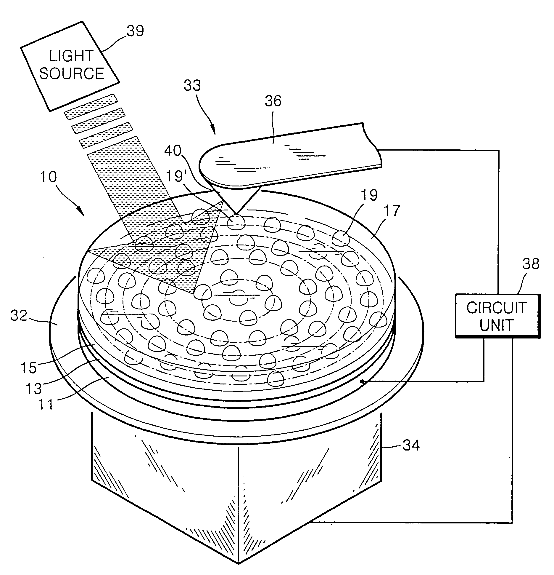
[0093]FIG. 5A is a diagram illustrating a method of writing data on the data storage medium according to the present invention using the data storage apparatus according to the present invention. A probe, which will be mentioned in the following paragraphs, is the same as the probe 33a shown in FIG. 4A.

[0094]Referring to FIG. 5A, the tip 40a of the probe 33a is placed over the data storage medium 10 to be in contact or out of contact with the surface of the data storage medium 10. Thereafter, voltages of the same magnitude are respectively applied to the source electrode 42, the drain electrode 44, and the tip 40a, and then photoelectrons of the photoelectron emission layer 15 are excited due to an electric field concentrated between the lower electrode 11 of the data storage medium 10 and the tip 40a. Thereaft...


PUM

PropertyMeasurementUnit
thicknessaaaaaaaaaa
photoelectron emissionaaaaaaaaaa
electric fieldaaaaaaaaaa

Abstract

A high-density data storage medium, a method of manufacturing the data storage medium, a high-density data storage apparatus, and methods of writing data on, and reading and erasing data from the data storage medium by using the data storage apparatus are provided. The data storage medium includes a lower electrode, an insulation layer deposited on the lower electrode, a photoelectron emission layer deposited on the insulation layer and having a plurality of protrusions from which photoelectrons are emitted due to collisions between the protrusions and photons, and a dielectric layer deposited on the photoelectron emission layer and storing the photoelectrons emitted from the photoelectron emission layer. The data storage apparatus includes a stage supporting a data storage medium, which includes a lower electrode, an insulation layer deposited on the lower electrode, a photoelectron emission layer deposited on the insulation layer and having a plurality of protrusions from which photoelectrons are emitted due to collisions between the protrusions and photons, and a dielectric layer deposited on the photoelectron emission layer and storing the photoelectrons emitted from the photoelectron emission layer, a scanner driving the stage, a probe placed over the data storage medium and including a tip forming an electric field with the data storage medium and a cantilever supporting the tip placed at its one end so as to maintain a predetermined distance between the data storage medium and the tip, a circuit unit applying a driving signal, a data write signal, and a data erase signal to the scanner and the probe and detecting a data read signal, and a light source irradiating light on the data storage medium.

Description

BACKGROUND OF THE INVENTION[0001]This application claims the priority of Korean Patent Application No. 2002-38881, filed on Jul. 5, 2002, in the Korean Intellectual Property Office, the disclosure of which is incorporated herein in its entirety by reference.[0002]1. Field of the Invention[0003]The present invention relates to a high-density data storage medium using emission of electrons caused by photons, a method of manufacturing the data storage medium, a data storage apparatus, and methods of writing data on and reading and erasing data from the data storage medium.[0004]2. Description of the Related Art[0005]In accordance with the increasing demand for small-sized electronic devices, such as mobile communications terminals or electronic notebooks, development of ultra small-sized high-density data storage media and apparatuses are becoming more necessary. However, it is not easy to manufacture small-sized hard disks and to increase the integration density of flash memories. The...

Claims


Application Information

Patent Timeline
Patent Type & Authority Patents(United States)
IPC IPC(8): H01J3/14G11B9/08G11B9/00G11B9/12G11B9/14G11B11/08G11B13/06G11C11/00G11C11/22H01J5/16H01L27/00H01L45/00
CPCB82Y10/00G11B9/14G11B9/149G11B9/1409G11B9/08G11B13/06G11B9/1472G11B11/08G11B9/12
Inventor HONG, SEUNG-BUMYOO, IN-KYEONGJUNG, JU-HWAN
Owner SAMSUNG ELECTRONICS CO LTD
Why Eureka
Try Eureka