High performance lateral bipolar transistor

a lateral bipolar transistor, high-performance technology, applied in the direction of galvano-magnetic devices, electrical equipment, semiconductor devices, etc., can solve the problems of reducing the contact resistance of lateral bipolar transistors, cmos devices may disappear, and cmos circuits may have a significant dynamic power dissipation factor, so as to reduce the contact resistance

Inactive Publication Date: 2007-02-06
ALTERA CORP
View PDF17 Cites 17 Cited by
  • Summary
  • Abstract
  • Description
  • Claims
  • Application Information

AI Technical Summary

Benefits of technology

[0016]Advantageously, the emitter and collector regions and the g...

Problems solved by technology

One characteristic of bipolar devices that has been considered a drawback for a long time is the higher static power dissipation than in CMOS devices.
However, this advantage of CMOS devices may disappear as their operating speed increases and the dynamic power dissipation of CMOS circuits becomes a significant factor.
Vertical bipolar transistors can exhibit excellent perform...

Method used


Image

  • High performance lateral bipolar transistor
  • High performance lateral bipolar transistor
  • High performance lateral bipolar transistor

Examples


Embodiment Construction

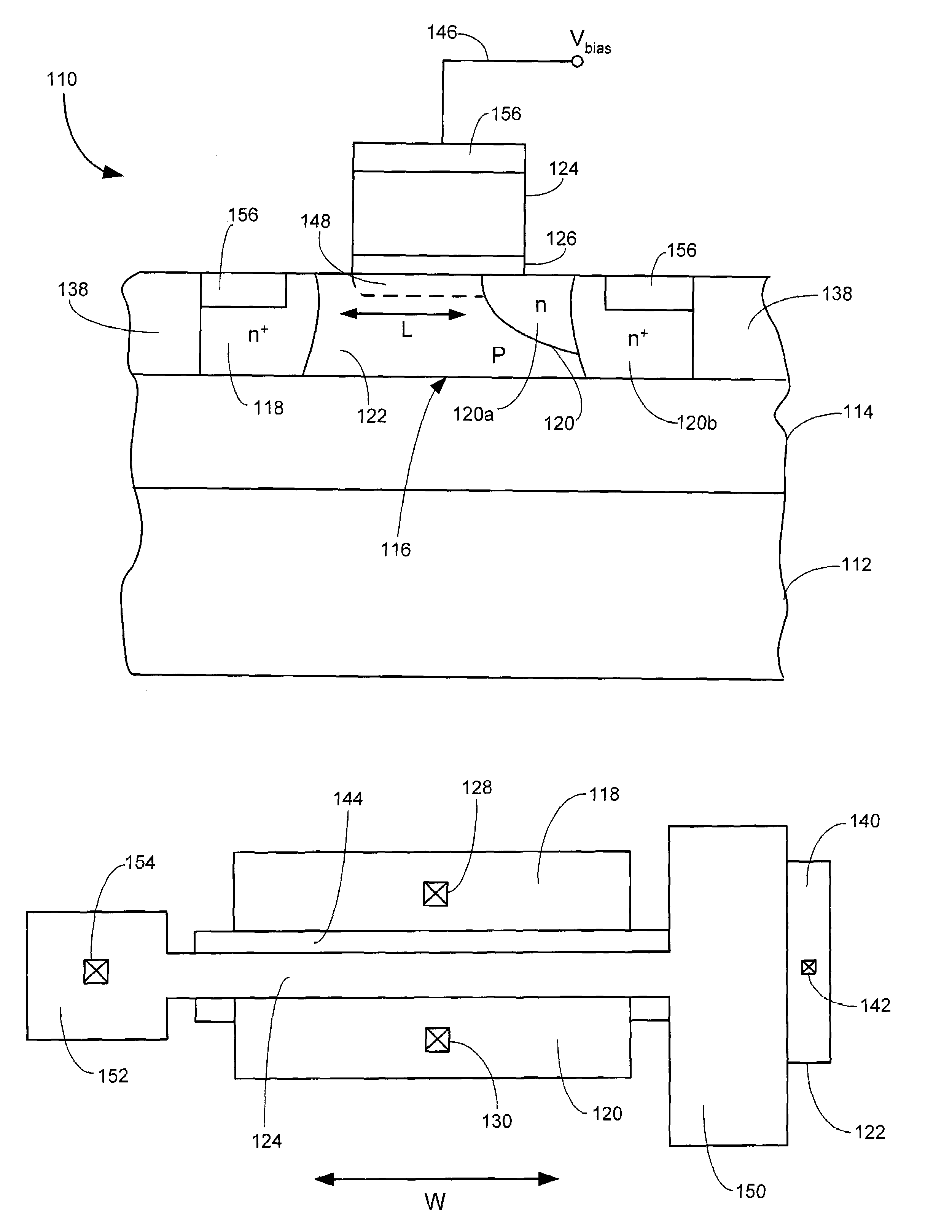
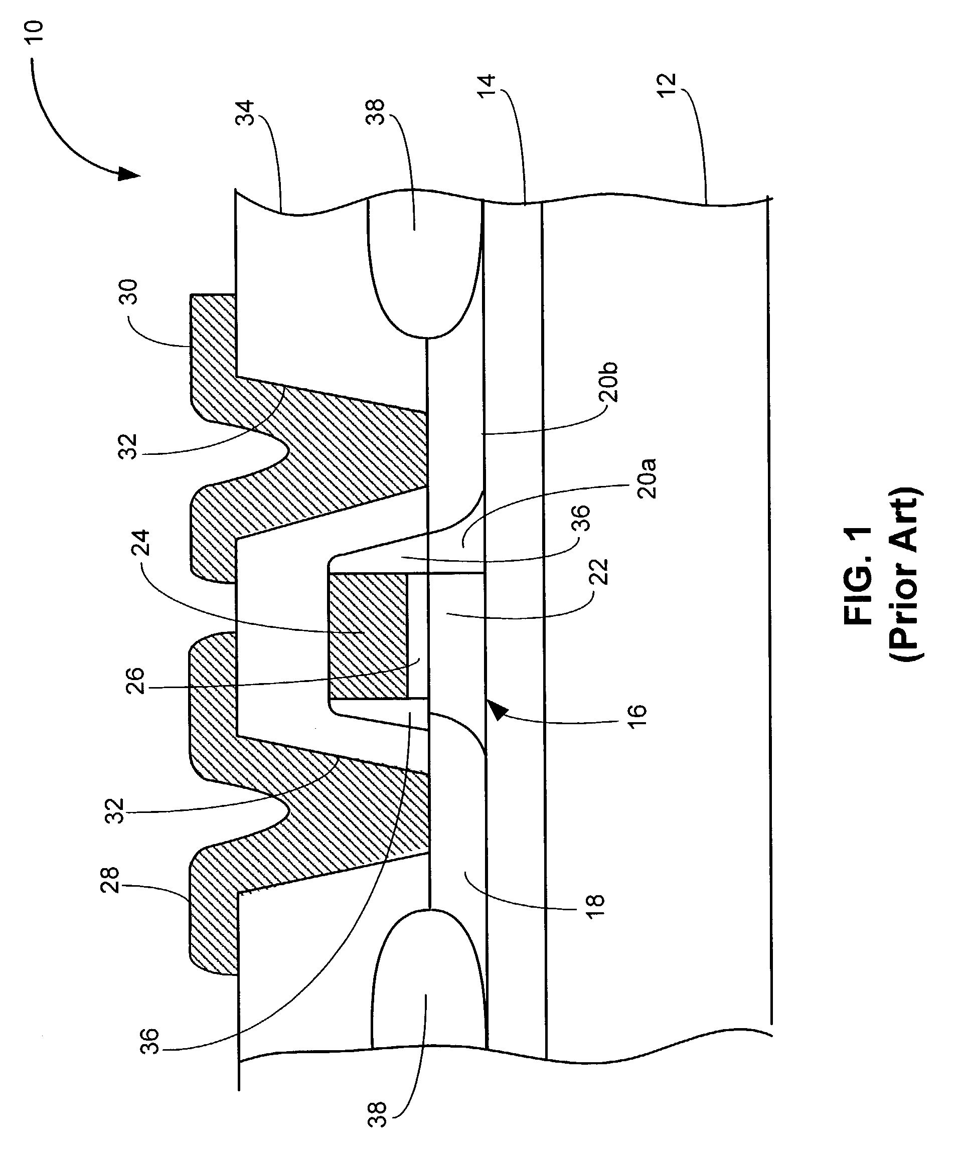
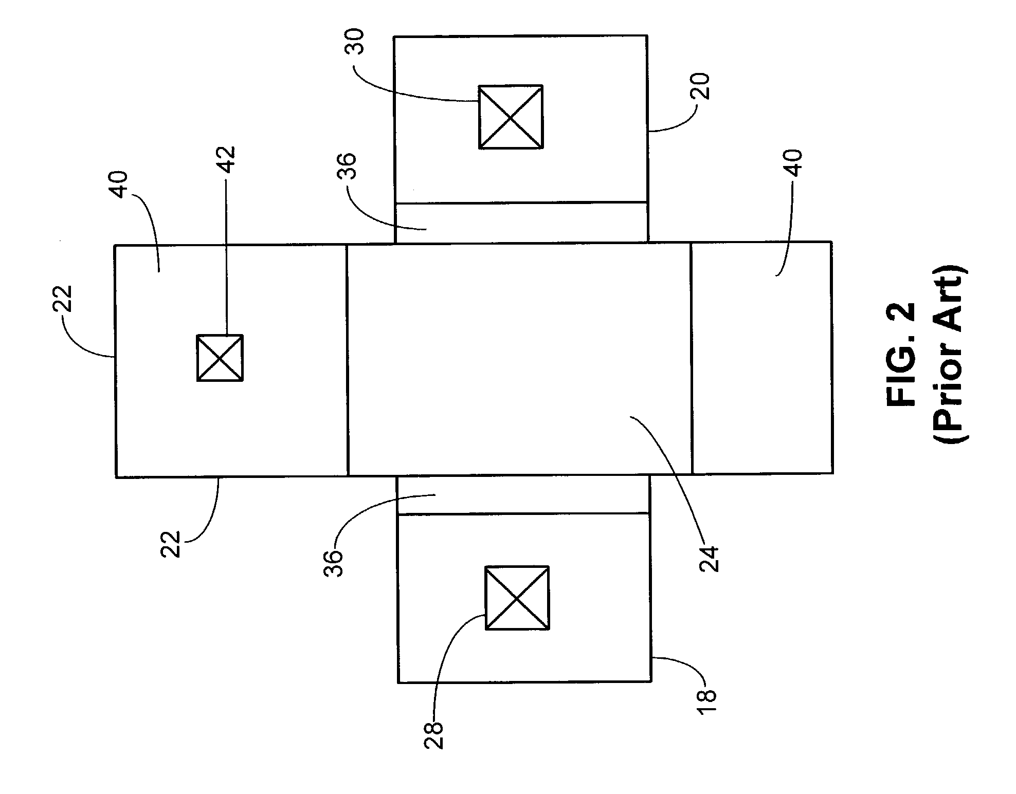
[0022]FIGS. 1 and 2 have already been described in relation to the prior art. In FIGS. 3 and 4, like or equivalent elements to the elements in FIGS. 1 and 2 are given like reference numerals, increased by 100.

[0023]The embodiment shown in FIGS. 3 and 4 features a lateral bipolar transistor 110 of npn type. A person of ordinary skills in the art, however, will easily appreciate that the principles of the present invention may equally be applied to a pnp-type transistor. Transistor 110 is fabricated in SOI technology and comprises a silicon substrate 112, an insulator 114 created in substrate 112 using, e.g., a SIMOX process, and a thin layer of single crystalline silicon 116 on insulator 114. Transistor 110 further comprises an emitter region 118 of n-conductivity type, a collector region 120 of n-conductivity type, and a base region 122 of p-conductivity type formed between emitter region 118 and collector region 120. Emitter region 118, base region 122 and collector region 120 are ...


PUM


Abstract

A lateral bipolar transistor includes an emitter region, a base region, a collector region, and a gate disposed over the base region. A bias line is connected to the gate for applying a bias voltage thereto during operation of the transistor. The polarity of the bias voltage is such as to create an accumulation layer in the base under the gate. The accumulation layer provides a low-resistance path for the transistor base current, thus reducing the base resistance of the transistor.

Description

BACKGROUND OF THE INVENTION[0001]The present invention relates generally to semiconductor devices and in particular to lateral bipolar transistors.[0002]From early on it has been the goal of integrated-circuit development to integrate on a chip as many components as possible. Integration allows fabrication of smaller and faster systems that dissipate less power. While CMOS (complementary metal-oxide-semiconductor) technology, which has become predominant in the fabrication of integrated circuits, particularly digital circuits, allows high integration levels and low-cost fabrication, bipolar technology has re-gained intensive attention in recent time due to such advantages over CMOS devices as higher speed, higher current density, lower noise and higher cutoff frequency. One characteristic of bipolar devices that has been considered a drawback for a long time is the higher static power dissipation than in CMOS devices. However, this advantage of CMOS devices may disappear as their op...

Claims


Application Information

Patent Timeline
IPC IPC(8): H01L29/00H01L27/082H01L29/82H01L43/00
CPCH01L29/0696H01L29/7394H01L29/7317H01L29/78624
Inventor RAHIM, IRFAN
Owner ALTERA CORP
Why Eureka
Try Eureka