
COF flexible printed wiring board and method of producing the wiring board

a flexible printed wiring and flexible technology, applied in the direction of printed circuit non-printed electric components association, lighting and heating apparatus, domestic cooling apparatus, etc., can solve the problems of unfavorable carrier tape deformation, deterioration of reliability and productivity, and the stoppage of a production apparatus, so as to improve reliability and productivity of the semiconductor chip mounting line

Inactive Publication Date: 2007-02-06
MITSUI MINING & SMELTING CO LTD
View PDF53 Cites 75 Cited by
  • Summary
  • Abstract
  • Description
  • Claims
  • Application Information

AI Technical Summary

Benefits of technology

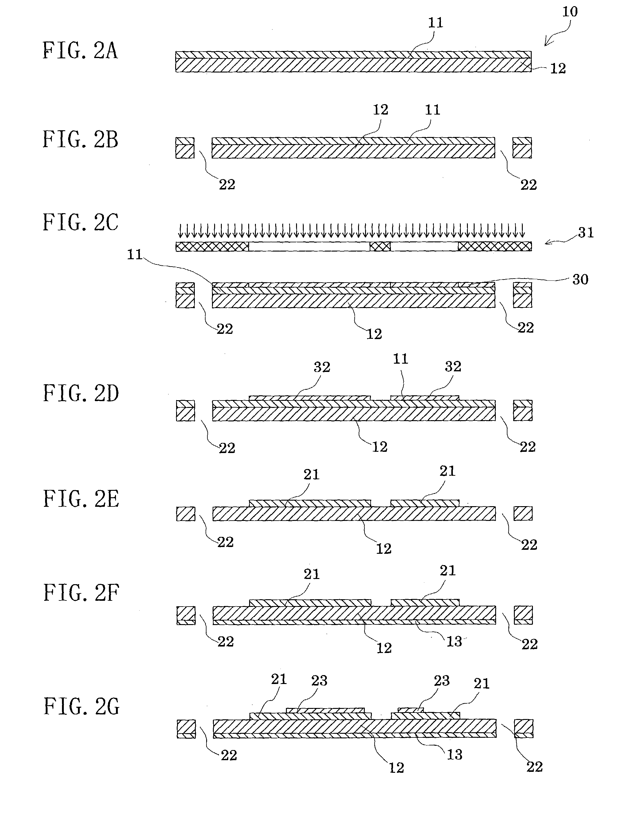
The present invention provides a COF flexible printed wiring board with an insulating layer that does not melt-adhere to a heating tool during mounting of semiconductor chips, thereby improving reliability and productivity of the semiconductor chip mounting line. The COF flexible printed wiring board includes a releasing layer that prevents staining of the heating tool caused by melt adhesion of the insulating layer. The releasing layer can be formed from a releasing agent containing a silicone series compound, a silane compound, or silica sol. The method of producing the COF flexible printed wiring board includes patterning the conductor layer through photolithography, and forming the releasing layer on the insulating layer, which is opposite to the mounting side of the semiconductor chip. The releasing layer can be formed from a releasing agent containing a siloxane compound, a silane compound, or silica sol.

Problems solved by technology

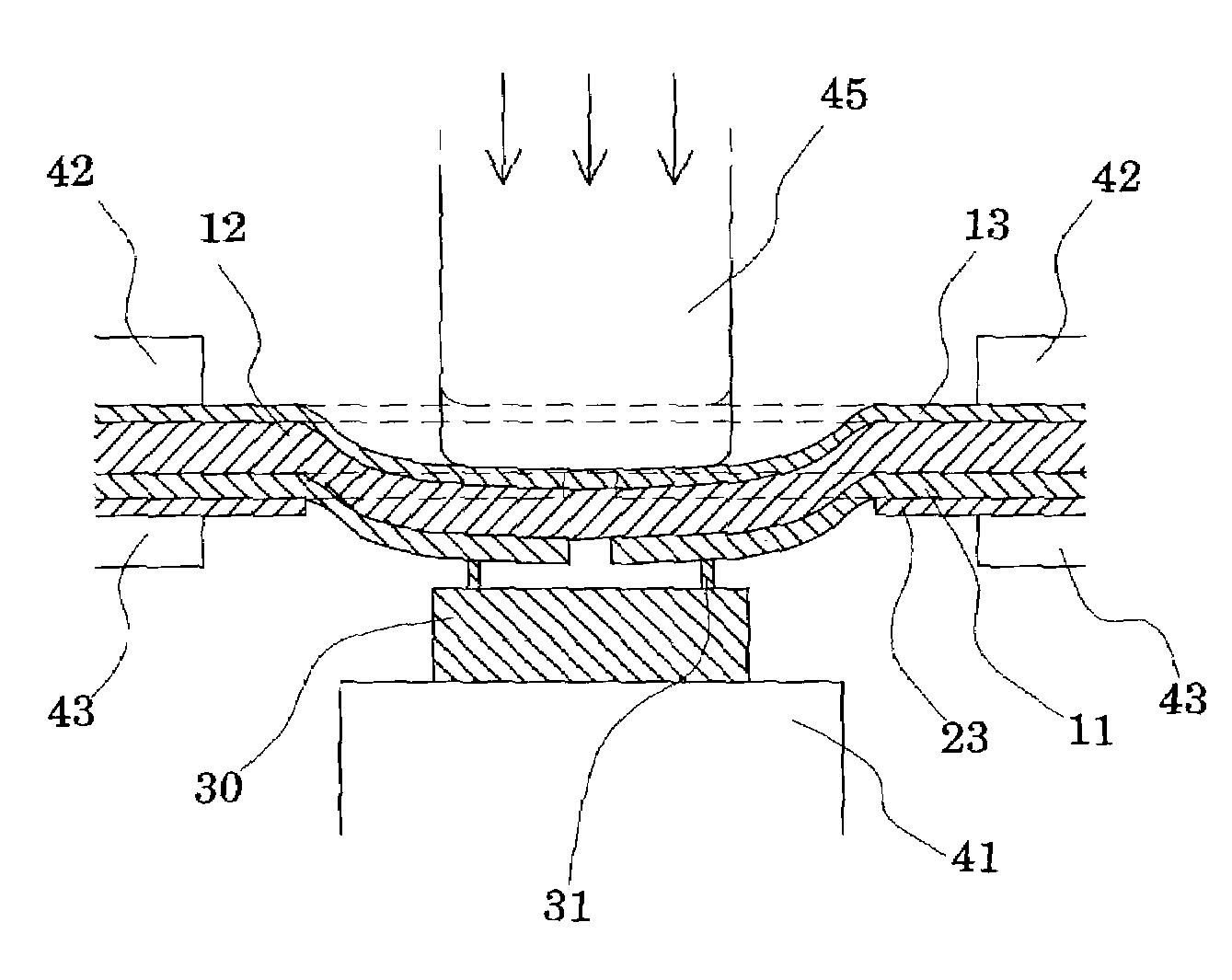
Since the insulating layer is heated to a considerably high temperature by the heating tool during mounting, a portion of the insulating layer is caused to adhere to the heating tool by melting, thereby causing stoppage of a production apparatus.
In addition, unfavorable deformation of the carrier tape occurs.
In the case where the insulating layer is melt-adhered to the heating tool, the heating tool is stained, thereby deteriorating reliability and productivity.

Method used


Image

  • COF flexible printed wiring board and method of producing the wiring board
  • COF flexible printed wiring board and method of producing the wiring board
  • COF flexible printed wiring board and method of producing the wiring board

Examples


examples 1a to 1d

[0099]A variety of commercially available polyimide film substrates; i.e., S'PERFLEX (trade name: product of Sumitomo Metal Mining Co., Ltd.; Example 1a), ESPANEX (trade name: product of Nippon Steel Chemical Co., Ltd.; Example 1b), NEOFLEX (trade name: product of Mitsui Chemicals, Inc.; Example 1c), and UPISEL (trade name: product of Ube Industries, Ltd.; Example 1d) were used to provide laminate films for producing a COF. A conductor layer of each laminate film was patterned by use of a photoresist. The entirety of the resultant pattern was tin-plated, and a silicone series resin (containing a silane compound), SR2411 (trade name: product of Dow Corning Toray Silicone Co., Ltd.), was applied to the backside of the film substrate. The coating was heated at 125° C. for one hour, to thereby form a COF film carrier tape having a releasing layer.

examples 2a to 2d

[0100]A variety of commercially available polyimide film substrates similar to those employed in Examples 1a to 1d; i.e., S'PERFLEX (trade name: product of Sumitomo Metal Mining Co., Ltd.; Example 2a), ESPANEX (trade name: product of Nippon Steel Chemical Co., Ltd.; Example 2b), NEOFLEX (trade name: product of Mitsui Chemicals, Inc.; Example 2c), and UPISEL (trade name: product of Ube Industries, Ltd.; Example 2d) were used to provide laminate films for producing a COF. A conductor layer of each laminate film was patterned by use of a photoresist. The entirety of the resultant pattern was tin-plated, and a silicone series resin (containing silazane), SEPA-COAT (trade name: product of Shin-Etsu Chemical Co., Ltd.), was applied to the backside of the film substrate. The coating was heated at 125° C. for one hour, to thereby form a COF film carrier tape having a releasing layer.

examples 3a to 3d

[0105]A variety of commercially available polyimide film substrates similar to those employed in Examples 1a to 1d; i.e., S'PERFLEX (trade name: product of Sumitomo Metal Mining Co., Ltd.; Example 3a), ESPANEX (trade name: product of Nippon Steel Chemical Co., Ltd.; Example 3b), NEOFLEX (trade name: product of Mitsui Chemicals, Inc.; Example 3c), and UPISEL (trade name: product of Ube Industries, Ltd.; Example 3d) were used to provide laminate films for producing a COF. A conductor layer of each laminate film was patterned by use of a photolithographic process, to thereby form a wiring pattern. The entirety of the wiring pattern was tin-plated, and subsequently a silicone series oil, SRX310 (trade name: product of Dow Corning Toray Silicone Co., Ltd.), was applied to the backside of the film substrate. The coating was heated at 125° C. for one hour, to thereby form a COF film carrier tape having a releasing layer.


PUM


Abstract

The present invention provides a COF flexible printed wiring board whose insulating layer is not melt-adhered to a heating tool, to thereby enhance reliability and productivity of a semiconductor chip mounting line, and also provides a method of producing the COF flexible printed wiring board. The COF flexible printed wiring board contains an insulating layer, a wiring pattern, on which a semiconductor chip being mounted, formed of a conductor layer provided on at least one side of the insulating layer and a releasing layer, wherein the releasing layer is formed from a releasing agent containing at least one species selected from a silane compound and silica sol and is provided on a surface of the insulating layer, which is opposite to the mounting side of the semiconductor chip.

Description

BACKGROUND OF THE INVENTION[0001]1. Field of the Invention[0002]The present invention relates to a COF (chip-on-film) flexible printed wiring board; e.g., a COF film carrier tape or a COF flexible printed circuit (FPC), for mounting electronic devices such as ICs and LSIs thereon. The invention also relates to a method of producing the COF flexible printed wiring board. The term “COF flexible printed wiring board” refers to a flexible printed wiring board onto which electronic devices (chips) are to be mounted. The term “COF film carrier tape” refers to a film substrate assuming the form of tape onto which electronic devices (chips) are to be mounted.[0003]2. Description of the Related Art[0004]Development of the electronics industry has been accompanied by sharp demand for printed-circuit boards for mounting electronic devices thereon, such as ICs (Integrated Circuits) and LSIs (Large-Scale Integrated circuits). Manufacturers have attempted to realize small-size, lightweight, and h...

Claims


Application Information

Patent Timeline
Patent Type & Authority Patents(United States)
IPC IPC(8): H01L23/02H01L23/498H05K1/18H05K3/28H05K3/34
CPCH01L23/4985H05K3/3494H05K3/28H01L2224/16H01L2924/01078H01L2924/01079H05K1/189H05K2203/1581H05K2201/10674H05K2203/0195H05K2203/066H01L2924/00014H01L2224/0401F25D5/02F25D2303/0822
Inventor SAKATA, KENHAYASHI, KATSUHIKO
Owner MITSUI MINING & SMELTING CO LTD
Learn More