Reduced area digital sigma-delta modulator

reduced area technology, applied in the field of implementing a digital sigma-delta modulator, can solve the problems of increasing system cost, increasing digital circuit cost, and reducing battery li

Active Publication Date: 2007-02-13
TEXAS INSTR INC
View PDF10 Cites 9 Cited by
  • Summary
  • Abstract
  • Description
  • Claims
  • Application Information

AI Technical Summary

Benefits of technology

[0015]Embodiments of the present invention achieve technical advantages as a sigma-delta modulator that can be used to set the frequency for an adjustable-frequency oscillator, and can be used in other applications such as bit width reduction for a digital signal or conversion of an analog signal into a digital format.
[0016]In accordance with a preferred embodiment, the invention solves the problem of producing a digital output signal with reduced bit width from a digital input signal using a sigma-delta modulator with minimal die area and less power dissipation, or producing a digital output signal from an analog input signal using a sigma-delta modulator, again with minimal die area and less power dissipation.
[0017]Embodiments of the present invention achieve technical advantages as a digital sigma-delta modulator that can produce an output signal with minimal signal processing delay. In a preferred embodiment, a digital sigma-delta modulator, comprises an input node coupled to an input signal and an output node producing an output signal. In a preferred embodiment, a plurality of integration stages is coupled in tandem between the input node and the output node, wherein the bit width of a signal in an integration stage coupled closer to the input node is wider than the bit width of a signal in an integration stage coupled closer to the output node. In a further preferred embodiment, the bit width of signals in the plurality of integration stages coupled in tandem between the input node and the output node is progressively reduced. In a further preferred embodiment, the plurality of integration stages comprises three integration stages. In a further preferred embodiment, the output signal is quantized to three bits.
[0019]In accordance with a preferred embodiment, a method of forming a digital sigma-delta modulator that can produce an output signal with minimal signal processing delay includes coupling an input node to an input signal and forming an output node to produce an output signal. In a preferred embodiment, the method includes coupling a plurality of integration stages in tandem between the input node and the output node, wherein the bit width of a signal in an integration stage coupled closer to the input node is wider than the bit width of a signal in an integration stage coupled closer to the output node. In a further preferred embodiment, the method includes progressively reducing the bit width of signals in the plurality of integration stages coupled in tandem between the input node and the output node. In a further preferred embodiment, the method includes using three integration stages for the plurality of integration stages. In a further preferred embodiment, the method includes quantizing the output signal to three bits.

Problems solved by technology

Modulators with higher orders of integration come with increased cost for the digital circuit as measured by indicators such as die area, gate count, signal processing delay, and power dissipation.
Adders generally comprise the slower digital elements in the modulator circuit and are usually the principal contributors to signal processing delay.
However, in low-power systems, particularly in portable systems, the digital sigma-delta modulator that drives the frequency divider generally consumes a substantial portion of the area and power of an IC (integrated circuit), which increases system cost and decreases battery life.

Method used


Image

  • Reduced area digital sigma-delta modulator
  • Reduced area digital sigma-delta modulator
  • Reduced area digital sigma-delta modulator

Examples


Embodiment Construction

[0030]The making and using of the presently preferred embodiments are discussed in detail below. It should be appreciated, however, that the present invention provides many applicable inventive concepts that can be embodied in a wide variety of specific contexts. The specific embodiments discussed are merely illustrative of specific ways to make and use the invention, and do not limit the scope of the invention.

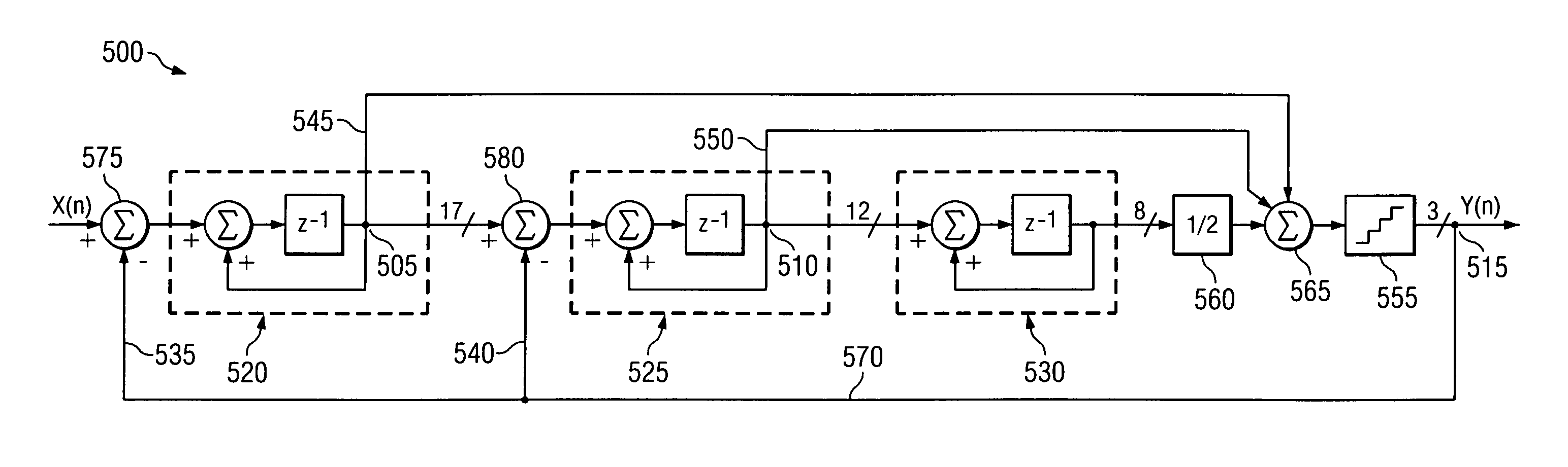
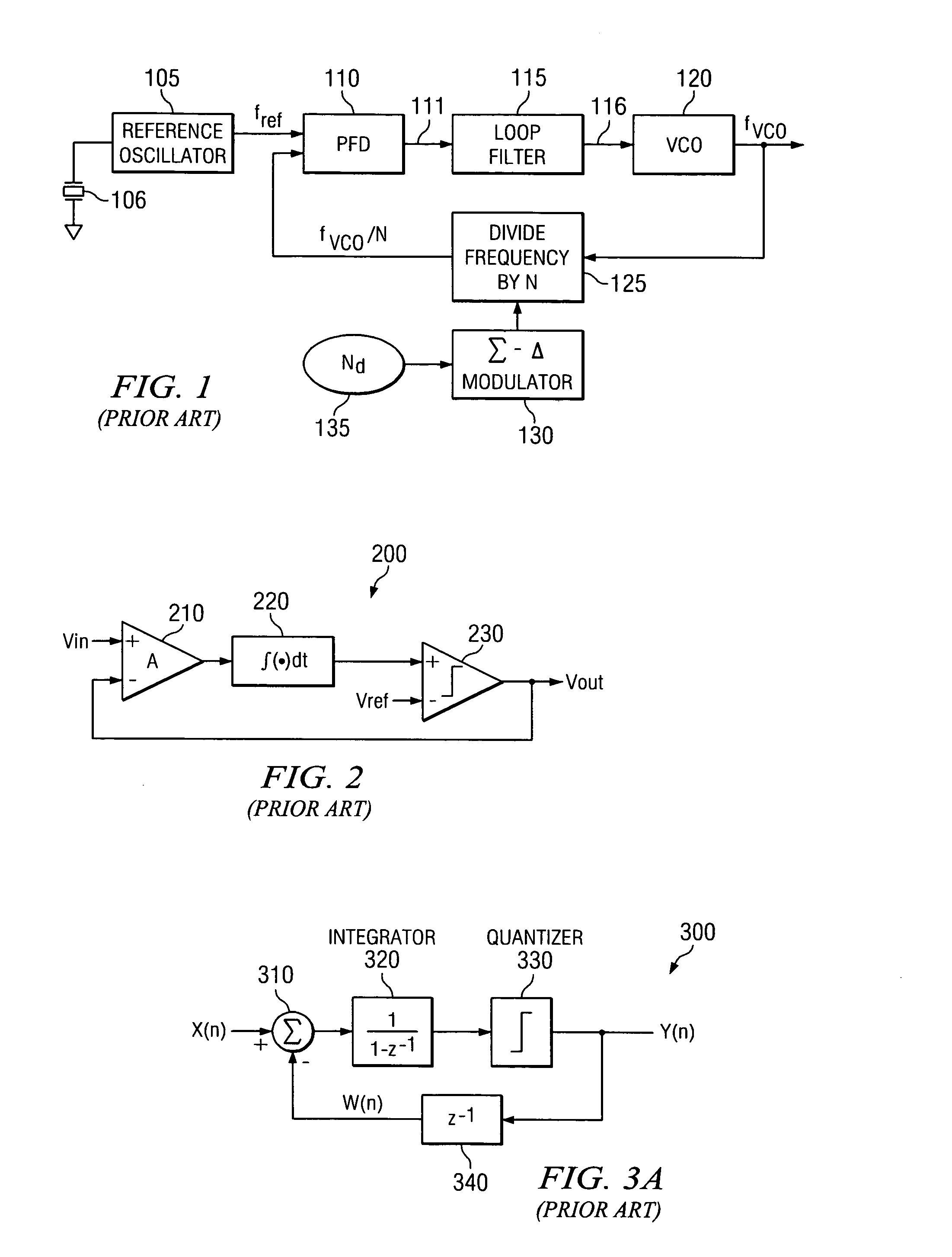
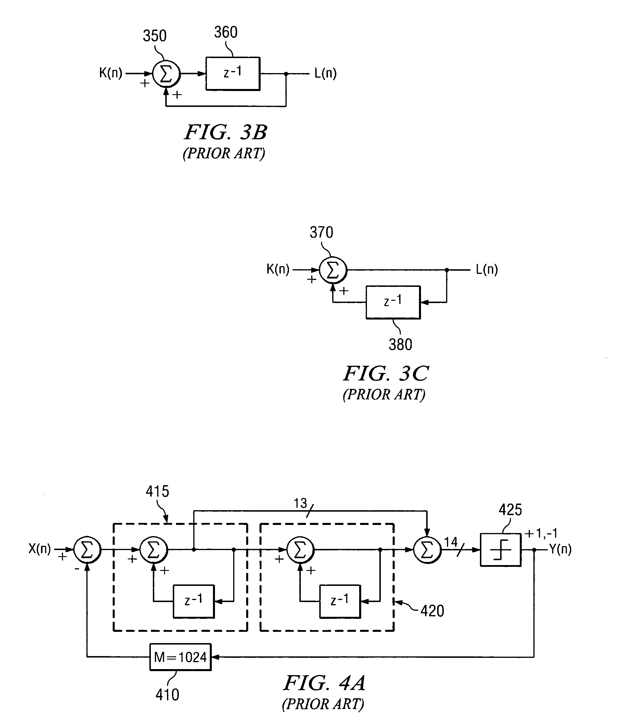
[0031]Embodiments of the present invention will be described with respect to preferred embodiments in a specific context, namely an apparatus and method using a sigma-delta modulator that can produce a digital output signal with reduced bit width from a digital input signal with minimal die area and low power dissipation, or produce a digital output signal from an analog input signal with minimal die area and low power dissipation. However, the use of this specific context is for illustrative purposes and does not limit the scope of the invention or the appended claims.

[0032]...


PUM


Abstract

A digital sigma-delta modulator requiring minimal die area and dissipating minimal power is formed with a plurality of integration stages coupled in tandem between an input node and an output node. The bit width of signals in the integration stages is progressively reduced from the first to the last integration stage without compromising modulator accuracy. A quantizer between the last integration stage and the output node provides the final reduction of signal bit width. The gain of the modulator feedforward and feedback paths are integer powers of two to further simplify the digital computation. In an exemplary implementation, three integration stages to form a third-order modulator are coupled in tandem between the input node and the output node. The gains of feedback and feedforward paths in one preferred embodiment are unity, and in some embodiments, one feedforward path has gain of 0.5.

Description

TECHNICAL FIELD[0001]This invention relates generally to producing a digital sampled-data sequence for a signal, and in particular, to a method and implementation for implementing a digital sigma-delta modulator such as for a frequency synthesizer.BACKGROUND[0002]Local oscillators are used in radio-frequency (RF) transmitters and receivers and in other applications to produce an adjustable-carrier or heterodyning frequency. An oscillator with an adjustable frequency enables a transceiver to communicate over a chosen channel. The local oscillator is generally implemented as a voltage-controlled oscillator (VCO) so that its frequency can be adjusted by a variable applied voltage. VCOs are generally implemented with a resonant tank circuit using a fixed inductor and a capacitor that is controlled with a voltage. Varactor diodes, which are back-biased semiconductor diodes, can be used to provide a voltage-controlled capacitance to adjust the resonant frequency of a resonant tank circuit...

Claims


Application Information

Patent Timeline
Patent Type & Authority Patents(United States)
IPC IPC(8): H03M3/00
CPCH03M7/3015H03M7/304H03M7/3037H03M7/3026
Inventor WILLIAMS, III, LOUIS ALBERTCAVALIERE, FRANCESCO
Owner TEXAS INSTR INC
Why Eureka
Try Eureka