Back-gate controlled read SRAM cell

a sram cell, back gate control technology, applied in static storage, digital storage, instruments, etc., can solve the problems of inability to scale the sram cell size in the future, inability to read sram cell size large, and inability to maintain the sram cell size. , to achieve the effect of improving the read stability of the sram cell, reducing the overhead area, and reducing the number of transistors

Inactive Publication Date: 2007-02-13
IBM CORP
View PDF6 Cites 61 Cited by
  • Summary
  • Abstract
  • Description
  • Claims
  • Application Information

AI Technical Summary

Benefits of technology

[0009]Another object of the present invention is to provide a new eight transistor SRAM cell structure which maintains advantages of ten transistor SRAM cells while reducing the area overhead.
[0010]A further object of the invention is to improve the read stability of a SRAM cell and to reduce the number of transistors in the cell using a back gate (or body) controlled read path.
[0011]These and other objectives are attained with an eight transistor static random access memory (SRAM) device, comprising first and second inverters, a first bit line, a first complement bit line, a pair of write access transistors, and a pair of read access transistors. Each of the first and second inverters includes a respective pair of transistors, and has a respective data node. Each of a first and a second of the access transistors has a source, a drain, a front gate, and a back gate. The first access transistor is coupled to the first bit line, and the second access transistor is coupled to the first complement bit line. The back gate of the first access transistor is coupled to the data node of the first inverter; and the back gate of the second access transistor is coupled to the data node of the second inverter. This increases the difference between the threshold voltages of the first and second access transistors.
[0012]The preferred embodiment of the invention, described in detail below, has a number of important advantages over previous known solutions. For instance, SRAM cells embodying this invention can have higher stability than the conventional six transistor SRAM, and the SRAM structure of the present invention has the smaller number of transistors than ten transistor SRAM while maintaining the same stability. Further, the present invention can use small differential bit line voltage split while the previous eight transistor SRAM uses single-ended bit line with large voltage swing. In addition, the preferred embodiment of this invention can be used in the future technology where the stability is hard to manage due to the process variations. This invention can also be used to reduce the area of multi-port register file design.

Problems solved by technology

The reduction of SNM threatens reliable functionality of SRAM, and, as a result, it may hinder the scaling of SRAM cell size in the future semiconductor technology to ensure the correct memory function.
While the use of a large SRAM cell gives higher stability so that it is possible to maintain correct memory read and write functionalities, the area penalty due to the large SRAM cell size is intolerable.
The 10T SRAM cell design approach also has large area consumption problem due to the increased number of transistors in a cell (from 6 to 10) although it is scalable to future technologies.
Although the 8T SRAM cell has the smaller area than the 10T SRAM cell has, single-end sensing scheme requires the higher bit line voltage development for correct sensing and it may limit the number of cells per sense amplifier.

Method used


Image

  • Back-gate controlled read SRAM cell
  • Back-gate controlled read SRAM cell
  • Back-gate controlled read SRAM cell

Examples


Embodiment Construction

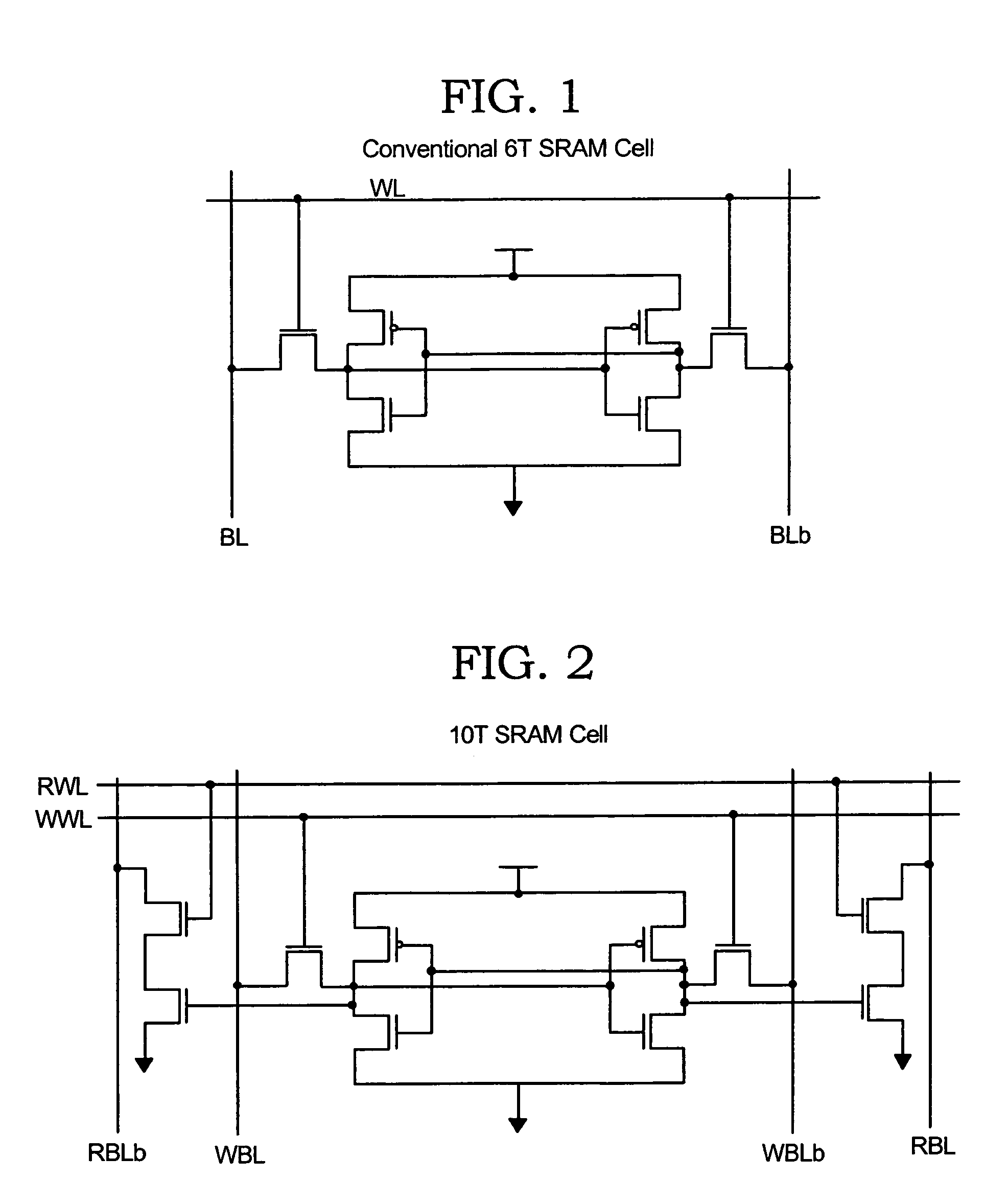
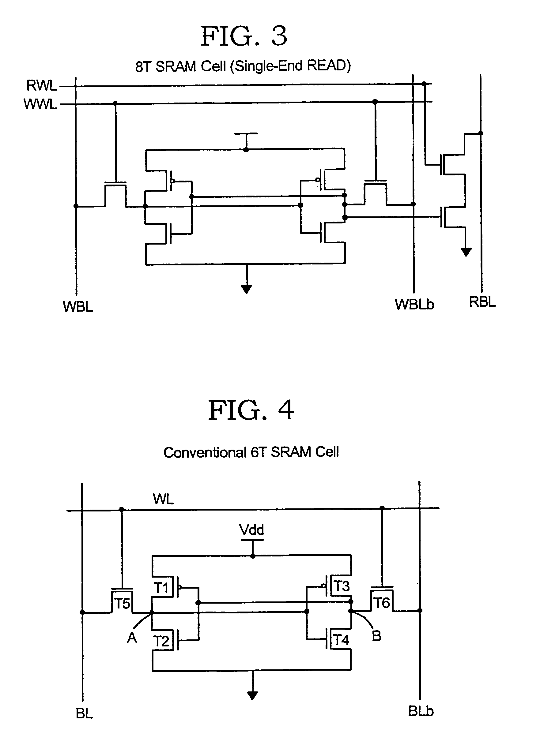
[0023]FIG. 4 illustrates a standard CMOS static RAM cell defined by six MOS transistors T1, T2, T3, T4, T5, and T6; of these transistors, transistors T1 and T2 are PMOS transistors while the remaining transistors are of the NMOS type. Transistors T1 and T3 are serially connected between Vdd and ground to form a first inverter with a data node A between the two transistors, and, in a similar manner, transistors T2 and T4 are likewise connected between Vdd and ground to form a second inverter with a data node B therebetween. The gates of the transistors of each inverter are connected together and cross-coupled to the data node of the other inverter. The transistor T5 is connected between the bit line BL and the data node A to provide data access thereto, and the transistor T6 is connected between the complementary bit line BLb and the data node B to similarly provide data access. The gates of the data access transistors T5 and T6 are connected to respective word lines WL; ancillary ci...


PUM


Abstract

An eight transistor static random access memory (SRAM)device includes first and second inverters, a first bit line, a first complement bit line, a pair of write access transistors, and a pair of read access transistors. Each of the first and second inverters includes a respective pair of transistors, and has a respective data node. Each of a first and a second of the access transistors has a source, a drain, a front gate, and a back gate. The first access transistor is coupled to the first bit line, and the second access transistor is coupled to the first complement bit line. The back gate of the first access transistor is coupled to the data node of the first inverter; and the back gate of the second access transistor is coupled to the data node of the second inverter. This increases the difference between the threshold voltages of the first and second access transistors.

Description

[0001]This invention was made with Government support under Contract No.: (NBCH3039004) awarded by (DARPA). The Government has cetain rights in this invention.BACKGROUND OF THE INVENTION[0002]1. Field of the Invention[0003]This invention generally relates to static random access memory (SRAM) devices; and more specifically, the invention relates to a back gate controlled SRAM device.[0004]2. Background Art[0005]An SRAM is a semiconductor device that allows data to be stored in a static manner—that is, in a manner that does not require any refresh cycles to maintain the stored data—and SRAMs are now a key component in microelectronic chips / applications. As the dimension of semiconductor technology scales down, the process variations including random doping fluctuation would be the crucial factor of the SRAM design. When large process variation for aggressively scaled device dimension occurs, threshold voltages of two neighbor transistors in a conventional 6-transistor (6T) SRAM cell,...

Claims


Application Information

Patent Timeline
Patent Type & Authority Patents(United States)
IPC IPC(8): G11C11/00
CPCG11C11/412
Inventor CHUANG, CHING-TE KENTKIM, JAE-JOONKIM, KEUNWOO
Owner IBM CORP
Why Eureka
Try Eureka