Semiconductor memory asynchronous pipeline

a technology of memory asynchronous pipeline and semiconductor memory, applied in the direction of memory adressing/allocation/relocation, information storage, transmission, etc., can solve the problems of different clock adjustments, delayed subsequent commands, and equal read latency

Inactive Publication Date: 2007-02-13
CONVERSANT INTPROP MANAGEMENT INC
View PDF19 Cites 13 Cited by
  • Summary
  • Abstract
  • Description
  • Claims
  • Application Information

AI Technical Summary

Benefits of technology

[0028]A still further aspect of the invention provides stages that are independent of the system clock thereby allowing the read data path to be run at any CAS latency which may be supported by a suitable resynchronizing output.

Problems solved by technology

This results in subsequent commands being delayed by the time it takes for the current data transfer to complete.
A regular clocked pipeline has the disadvantage that the read latency will be equal to the delay of the slowest pipeline stage (i.e. longest delay) multiplied by the number of pipeline stages.
A disadvantage of this scheme is that different adjustments to the clock are needed for each CAS latency supported by the chip.
Also, architecture changes can have a large impact on the breakdown of the latency stages, requiring designers to readjust all the clocks to accommodate the new division of latency stages.
Furthermore there are a limited number of places where a latency stage can be inserted without adding extra latency or chip area.
Multiple latency stages have a disadvantage in that not all latency stages will be equal in the time needed for signals to propagate through the stage.
Another complication is the need to enable or disable latency stages depending on the CAS latency at which the chip has been programmed to operate.
This data path skew makes it difficult to safely resynchronize the retrieved data in a wave pipeline implementation.

Method used


Image

  • Semiconductor memory asynchronous pipeline
  • Semiconductor memory asynchronous pipeline
  • Semiconductor memory asynchronous pipeline

Examples


Embodiment Construction

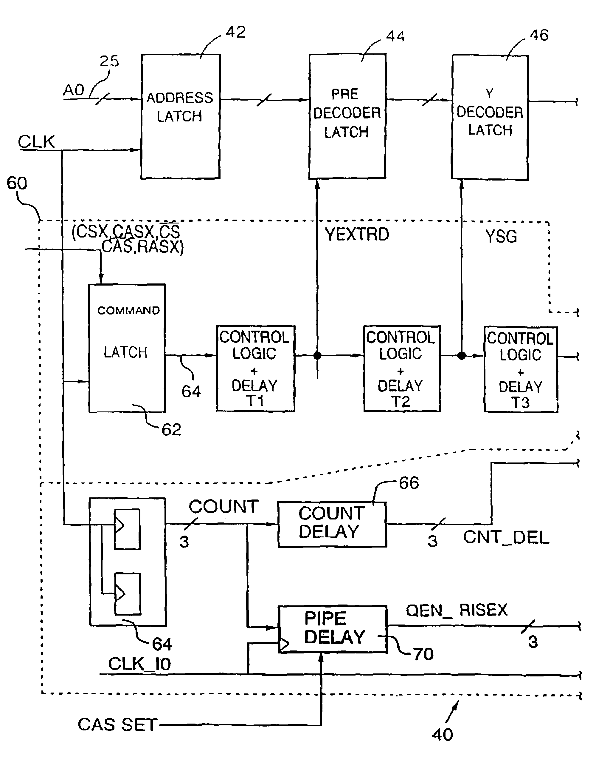
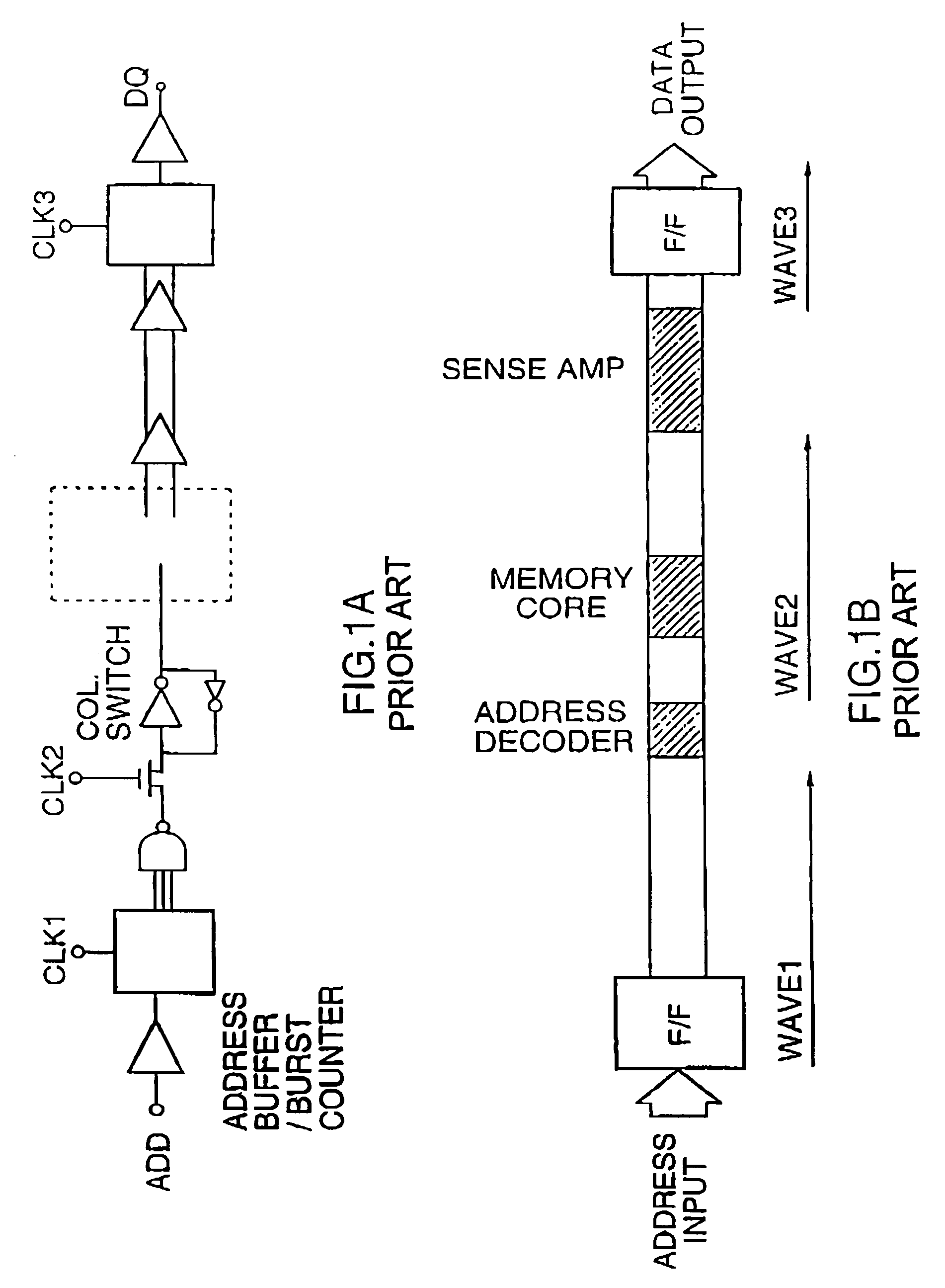
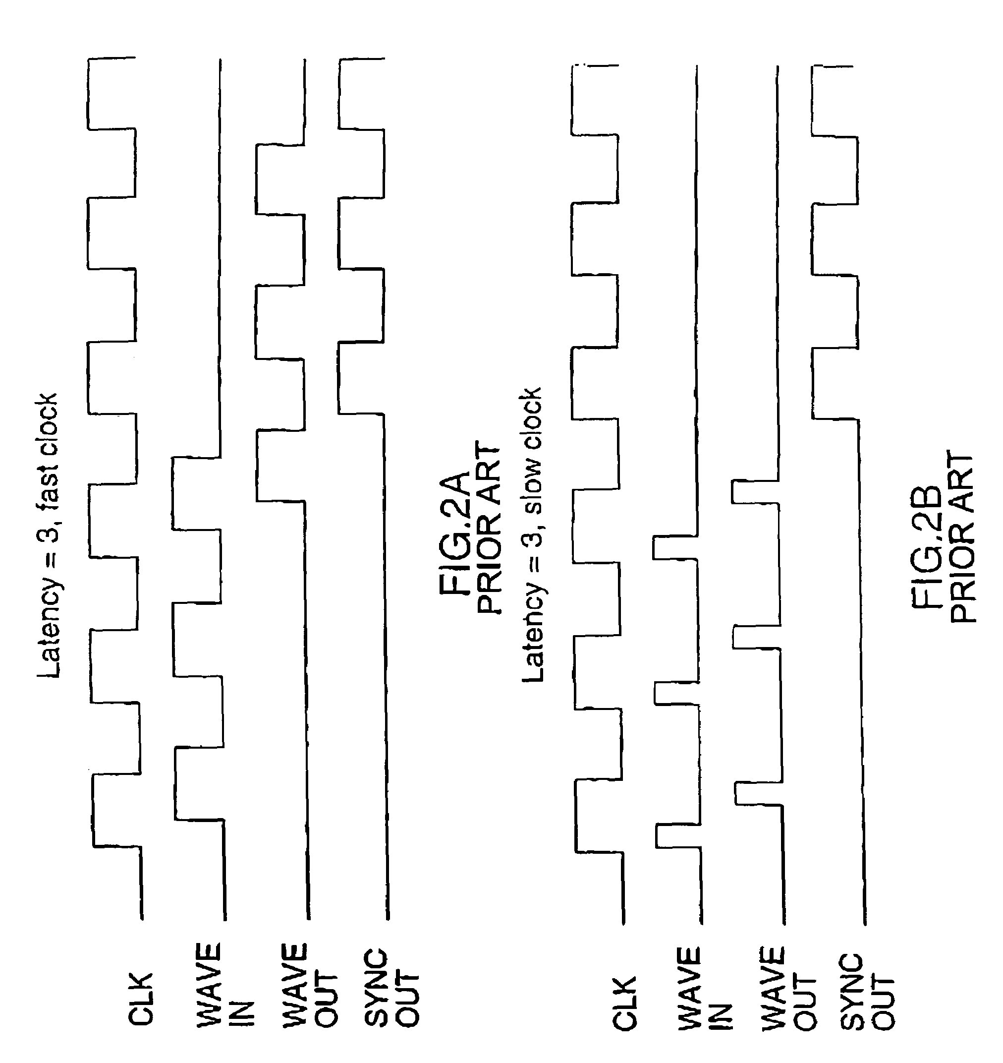
[0040]In the following discussion, like numerals refer to like elements in the figures and signals asserted low are indicated interchangeably with an x or an overscore associated with the corresponding signal name. Referring now to FIG. 3, a schematic diagram of a pipelined semiconductor memory according to a generalized embodiment of the invention is shown generally by numeral 20. The memory includes a core memory array 22 having a read path 24, defined between an address input port 25 and a data output 32. The read path 24 is broken up into latency stages 27, each of which is latched by respective asynchronous control signals 28. A synchronizing circuit 30 is coupled to the last latency stage of the read path in order to resynchronize the data to the system clock CLK at output 32 of the read path. The data is synchronized to the system clock CLK a predetermined number of clock cycles after the application of an address signal A to the address input 25, i.e. depending on the CAS la...


PUM


Abstract

An asynchronously pipelined SDRAM has separate pipeline stages that are controlled by asynchronous signals. Rather than using a clock signal to synchronize data at each stage, an asynchronous signal is used to latch data at every stage. The asynchronous control signals are generated within the chip and are optimized to the different latency stages. Longer latency stages require larger delays elements, while shorter latency states require shorter delay elements. The data is synchronized to the clock at the end of the read data path before being read out of the chip. Because the data has been latched at each pipeline stage, it suffers from less skew than would be seen in a conventional wave pipeline architecture. Furthermore, since the stages are independent of the system clock, the read data path can be run at any CAS latency as long as the re-synchronizing output is built to support it.

Description

CROSS REFERENCE TO RELATED APPLICATIONS[0001]This application is a Continuation Application from U.S. application Ser. No. 10 / 290,317 filed Nov. 8, 2002, now U.S. Pat. No. 6,772,312, which in turn is a Continuation Application of from U.S. application Ser. No. 09 / 129,878 filed Aug. 6, 1998 now U.S. Pat. No. 6,539,454, which claims priority from Canadian Patent Application No. 2,233,789, filed Apr. 1, 1998.[0002]The present invention relates to semiconductor memories and, more particularly, to a pipelined data access in a dynamic random access memory.BACKGROUND OF THE INVENTION[0003]In conventional non-pipelined dynamic random access memories (DRAMs) a data transfer to and from the memory is performed in sequence. That is, when a read or a write command is received and an address is made available, the data transfer according to either a read or write command is performed in its entirety before another command is accepted by the memory. This results in subsequent commands being delay...

Claims


Application Information

Patent Timeline
Patent Type & Authority Patents(United States)
IPC IPC(8): G06F12/00G06F1/00G06F1/12G11C8/00G11C8/18G11C11/407G11C7/10G11C11/409
CPCG11C7/1039G11C7/1051G11C7/106G11C11/4076G11C7/22G11C7/222G11C7/1072
Inventor MES, IAN
Owner CONVERSANT INTPROP MANAGEMENT INC
Why Eureka
Try Eureka