Eureka AIR delivers breakthrough ideas for toughest innovation challenges, trusted by R&D personnel around the world.

Display device and manufacturing method thereof

a technology manufacturing methods, applied in static indicating devices, instruments, horology, etc., can solve the problems and achieve the effect of deteriorating electrical reliability of thin film transistors

Active Publication Date: 2007-02-20
PANASONIC LIQUID CRYSTAL DISPLAY CO LTD +1
View PDF5 Cites 2 Cited by
  • Summary
  • Abstract
  • Description
  • Claims
  • Application Information

AI Technical Summary

Benefits of technology

[0010]These constitutions are provided for reducing the interface level density of the thin film transistor or for obtaining other advantageous effects.
[0011]The liquid crystal display device having these thin film transistors formed of polysilicon is, usually, configured such that a scanning signal drive circuit which supplies scanning signals to gate signal lines or a video signal drive circuit which supplies video signals to drain signal lines and the like are formed on one substrate, while semiconductor layers of MIS (Metal Insulator Semiconductor) transistors which are incorporated into these peripheral circuits are also formed of polysilicon. This is because the MIS transistors can be formed along with the formation of the thin film transistors on pixel regions.BRIEF SUMMARY OF THE INVENTION
[0012]However, when at least one layer of insulation film which is formed by a CVD method, for example, is provided as the gate insulation film of the thin film transistor formed of polysilicon as described above and the insulation film is directly brought into contact with a polysilicon layer, for example, it has been found that a following drawback arises.
[0013]That is, when the insulation film is formed by the CVD method, carbons contained in a raw material gas (TEOS, TMS or the like) thereof are trapped in the film and hence, it is confirmed that a level of an interface with the polysilicon layer is elevated and fixed charges in the insulation film are increased whereby the electrical reliability of the thin film transistor is deteriorated.
[0014]The present invention has been made under such circumstances and it is an object of the present invention to provide a display device which can obviate the elevation of a level of an interface of an insulation film with respect to a polysilicon layer in a thin film transistor and, at the same time, can obviate the increase of fixed charges in the insulation film.

Problems solved by technology

However, when at least one layer of insulation film which is formed by a CVD method, for example, is provided as the gate insulation film of the thin film transistor formed of polysilicon as described above and the insulation film is directly brought into contact with a polysilicon layer, for example, it has been found that a following drawback arises.
That is, when the insulation film is formed by the CVD method, carbons contained in a raw material gas (TEOS, TMS or the like) thereof are trapped in the film and hence, it is confirmed that a level of an interface with the polysilicon layer is elevated and fixed charges in the insulation film are increased whereby the electrical reliability of the thin film transistor is deteriorated.

Method used


Image

  • Display device and manufacturing method thereof
  • Display device and manufacturing method thereof
  • Display device and manufacturing method thereof

Examples


Embodiment Construction

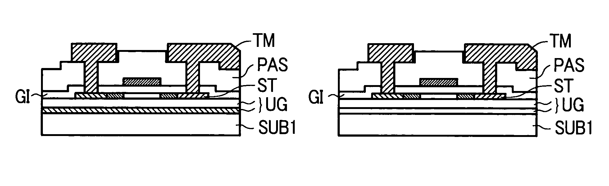
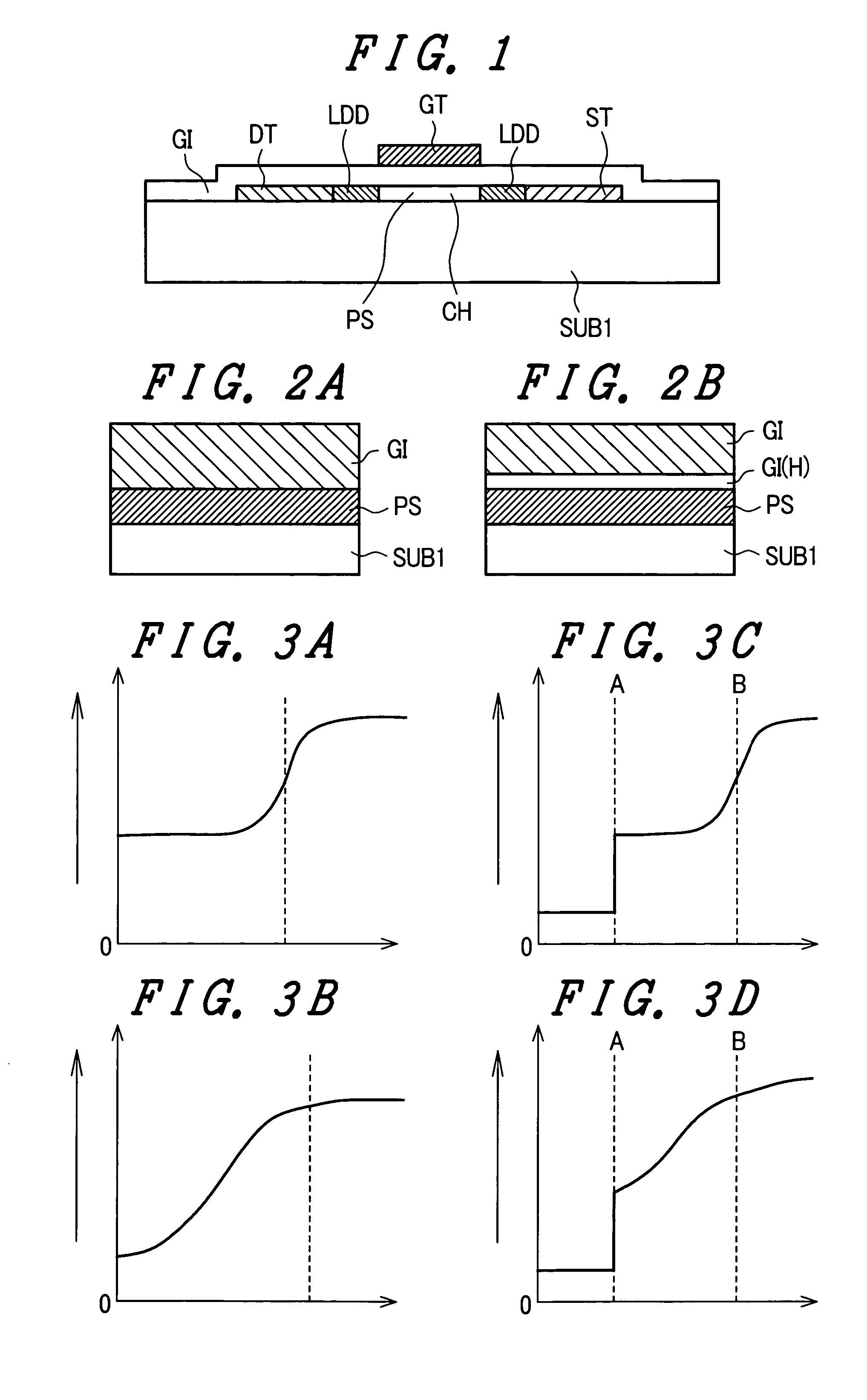
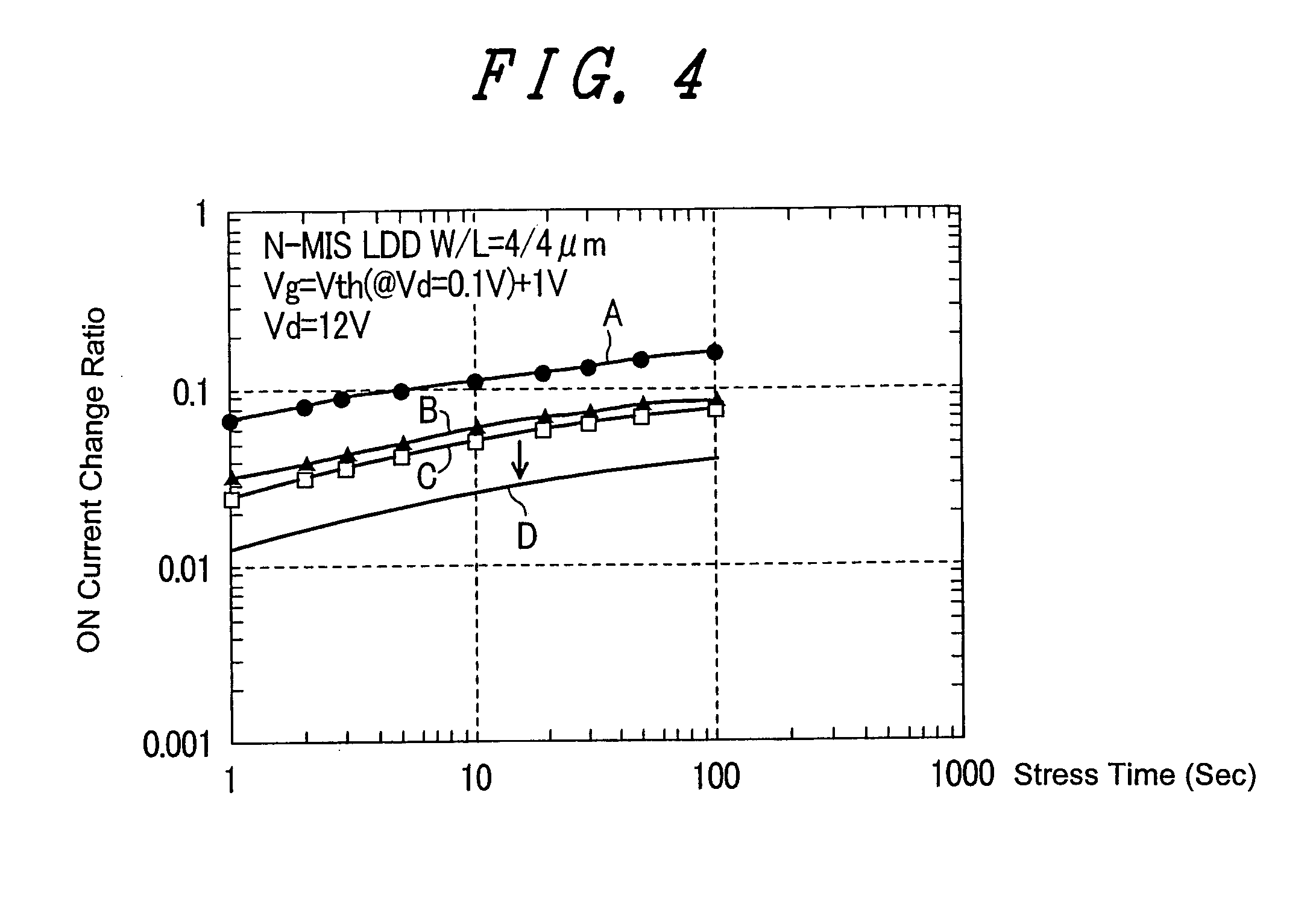
[0057]Preferred embodiments of a display device according to the present invention are explained in detail in conjunction with drawings.

>

[0058]FIG. 15 is an equivalent circuit diagram showing one embodiment of a liquid crystal display device, for example.

[0059]In the drawing, there are provided a pair of transparent substrates SUB1, SUB2 which are arranged to face each other in an opposed manner with liquid crystal therebetween, wherein the liquid crystal is sealed by a sealing material SL which also performs a function of fixing another transparent substrate SUB2 to one transparent substrate SUB1.

[0060]On a liquid-crystal-side surface of one transparent substrate SUB1 which is surrounded by the sealing material SL, gate signal lines GL which extend in the x direction and are arranged in parallel in the y direction and drain signal lines DL which extend in the y direction and are arranged in parallel in the x direction are formed.

[0061]Regions which are surrounded by the respective ...


PUM

PropertyMeasurementUnit
sizeaaaaaaaaaa
thicknessaaaaaaaaaa
widthaaaaaaaaaa

Abstract

In a display device including thin film transistors formed on an insulation substrate, the thin film transistor includes a semiconductor layer, a gate electrode and a gate insulation film which is interposed between the semiconductor layer and the gate electrode. The gate insulation film includes at least one layer of deposition film which is deposited by a deposition method, and the carbon concentration of the gate insulation film which is formed without interposing other deposition film deposited by a deposition method between the one deposition film and the semiconductor layer has the distribution in which the carbon concentration is smaller at a side close to the semiconductor layer than at a side remote from the semiconductor layer. Due to such a constitution, it is possible to obviate the elevation of a level of an interface of the insulation film with respect to a poly silicon layer and it is also possible to obviate an increase of fixed charges in the inside of the insulation film in the thin film transistor.

Description

BACKGROUND OF THE INVENTION[0001]1. Field of the Invention[0002]The present invention relates to a display device, and more particularly to a display device which is referred to as an active matrix type display device.[0003]2. Description of the Related Art[0004]For example, a liquid crystal display device of this type is configured such that a pair of substrates are arranged to face each other with liquid crystal therebetween and, on a liquid-crystal-side surface of one of these substrates, g ate signal lines which extend in the x direction and are arranged in parallel in the y direction and drain signal lines which extend in the y direction and are arranged in parallel in the x direction are formed, wherein respective regions which are surrounded by these respective signal lines constitute pixel regions.[0005]Then, each pixel region includes at least a thin film transistor which is driven in response to a scanning signal from the one-side gate signal line and a pixel electrode to ...

Claims


Application Information

Patent Timeline
Patent Type & Authority Patents(United States)
IPC IPC(8): H01L29/15G02F1/1368C23C16/455H01L21/316H01L21/336H01L21/77H01L21/84H01L27/12H01L29/49H01L29/786H01L51/50
CPCH01L29/4908H01L27/12H01L27/1214
Inventor KAMO, TAKAHIROITOGA, TOSHIHIKOKAITOH, TAKUOOHKURA, MAKOTO
Owner PANASONIC LIQUID CRYSTAL DISPLAY CO LTD
Why Eureka
Eureka Blog
Learn More