
Exposure apparatus and device manufacturing method

a technology of equipment and manufacturing method, applied in the field of equipment, can solve the problems of limiting the number of units produced per model, increasing mask cost, complicated phase shift mask, etc., and achieves the effects of simple structure, high throughput, and easy operation

Inactive Publication Date: 2007-02-20
CANON KK
View PDF8 Cites 20 Cited by
  • Summary
  • Abstract
  • Description
  • Claims
  • Application Information

AI Technical Summary

Benefits of technology

This approach results in a high-throughput, cost-effective maskless exposure apparatus capable of producing semiconductor devices with submicron resolution, reducing production time and mask costs, and improving economic efficiency by eliminating the need for expensive phase shift masks.

Problems solved by technology

Various consumers' demands require the manufacture of various products, and limit the number of units produced per model.
The phase shift mask is more complicated and thus more expensive than a conventional binary mask.
However, when the number of produced system LSIs are low, a mask cost increases, which makes the device and mask expensive, such as the phase shift mask.
The 1 / 10,000 reduction optical system is less feasible, and it takes an enormous time to connect patterns on the overall surface of a semiconductor wafer having a diameter of 300 mm for mass production.
However, the gray scale technology disclosed in International Application, Domestic Publication No. 2002-506233 needs an analog-to-digital conversion for each of a million of micro mirrors, and calibrates each micro mirror, causing a very complex and large system.
The gray scale technology disclosed in Japanese Patent Application, Publication No. 2003-243300 complicates an optical system that synthesizes images formed by the distant spatial modulation elements, and has difficulties in assembly and adjustment.
However, the current wafer stage speed has already reached the upper limit, and the improved throughput using the improved wafer stage speed cannot be expected.

Method used


Image

  • Exposure apparatus and device manufacturing method
  • Exposure apparatus and device manufacturing method
  • Exposure apparatus and device manufacturing method

Examples


Embodiment Construction

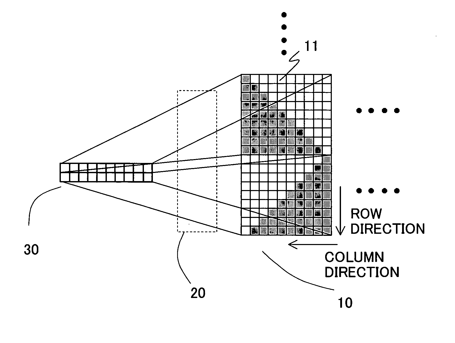
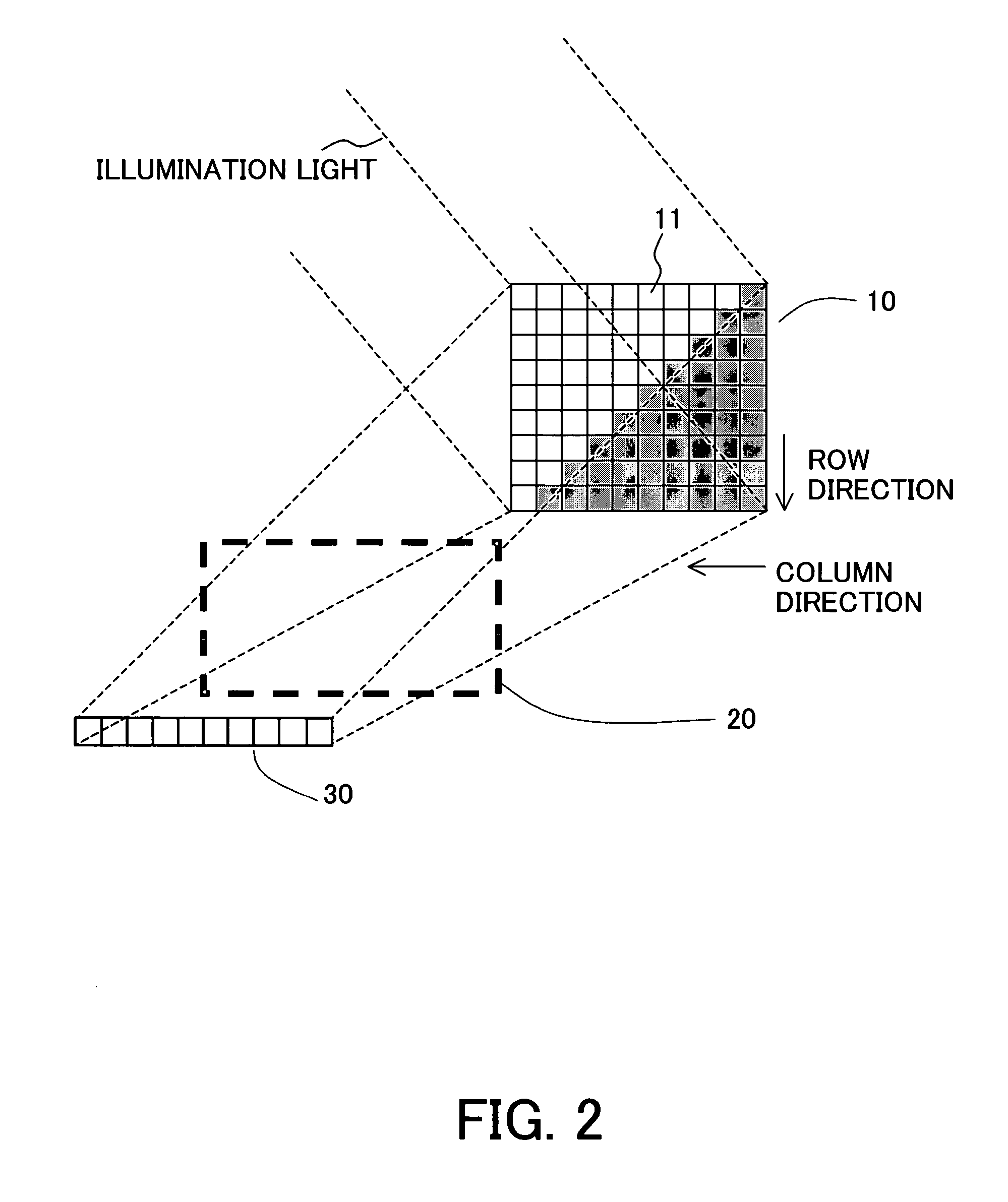
[0037]Referring now to the accompanying drawings, a description will be given of an exposure apparatus according to one aspect of the present invention. Like elements in each figure are designated by the same reference numerals, and a description thereof will be omitted.

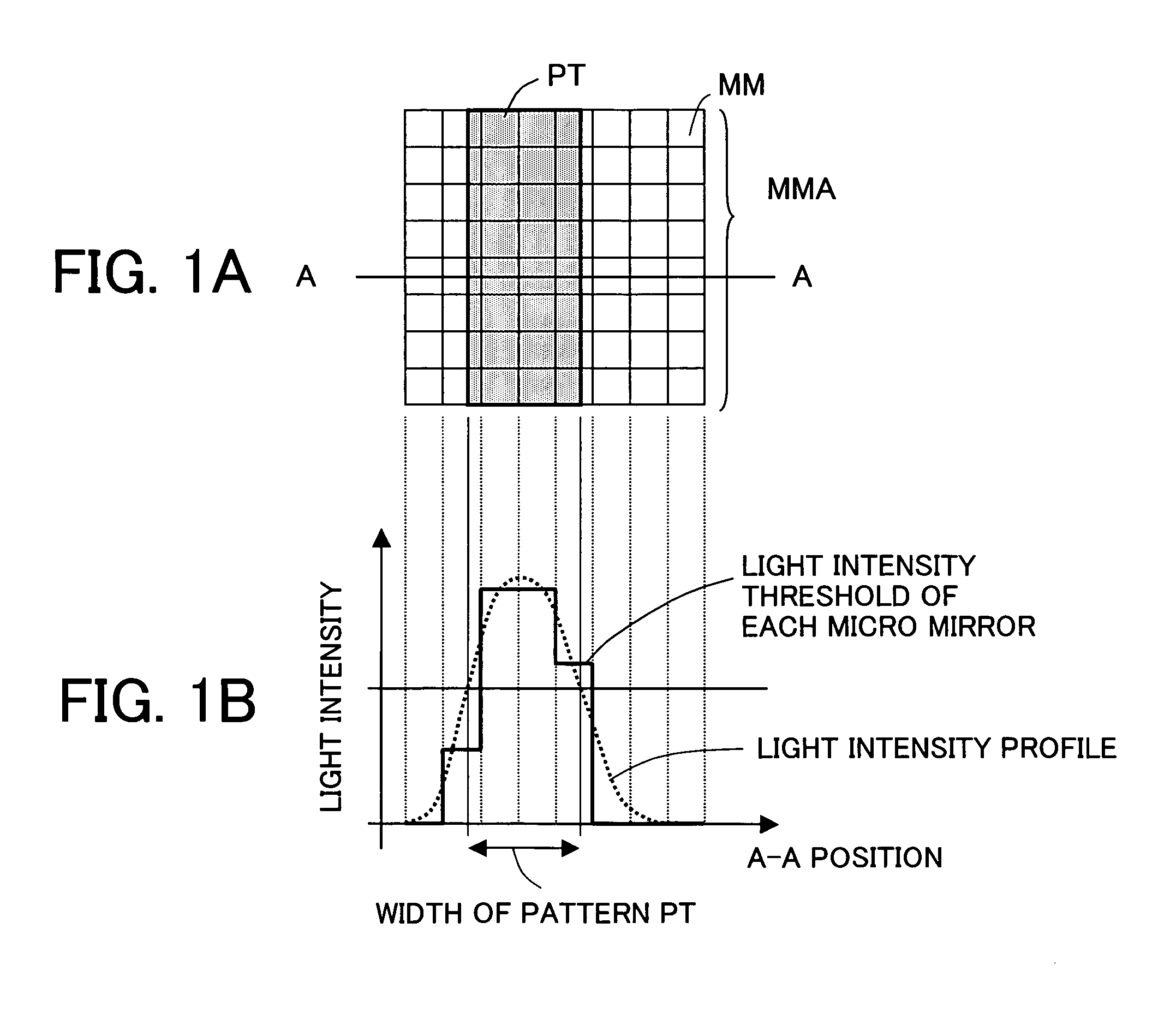
[0038]A description will now be given of the gray scale for better understanding of the inventive exposure apparatus. FIG. 1A is a plane view of a micro-mirror array (“MAA”) that has sixty-four micro mirrors (“MM”) or pixels, i.e., eight long by eight broad. A rectangular area PT denotes a pattern to be formed. As shown in FIG. 1A, an outline of the pattern PT does not accord with outlines of the MMs.

[0039]FIG. 1B is a light intensity distribution of the MMA shown in FIG. 1A, where an ordinate axis denotes the light intensity and an abscissa axis denotes a MMA's position. The solid line denotes the light intensity of each MM, and a broken line denotes a projected intensity profile.

[0040]The original intensity distrib...


PUM


Abstract

An exposure apparatus includes a projection optical system for projecting a multigradation pattern onto an object, a spatial modulation element that includes plural, two-dimensionally arranged pixels, and forms an optical image by binary control over each pixel, and a superposing optical system for forming the multigradation pattern by superposing the optical images for each row and / or for each column.

Description

[0001]This application claims a benefit of priority based on Japanese Patent Application No. 2004-311010, filed on Oct. 26, 2004, which is hereby incorporated by reference herein in its entirety as if fully set forth herein.BACKGROUND OF THE INVENTION[0002]The present invention relates generally to an exposure apparatus, and more particularly to an exposure apparatus and method used to manufacture various devices including semiconductor chips, a display device, a sensing device such as a magnetic head, an image pickup device such as a CCD, and a fine pattern for micromechanics. The present invention is suitable, for example, for a maskless exposure apparatus that utilizes a spatial modulation element, such as a micro-mirror array, and dispenses with a mask as an original.[0003]Due to the demand by the large personal computer (“PC”) market, the fine processing of the semiconductor integrated circuits (“ICs”) has rapidly developed, and the design rule of 90 nm has been achieved. Many ...

Claims


Application Information

Patent Timeline
Patent Type & Authority Patents(United States)
IPC IPC(8): G03B27/42G03B27/54
CPCG03F7/70291G03F7/70283
Inventor KASUMI, KAZUYUKIOTA, HIROHISAKAWAKAMI, EIGONAKAMURA, TAKASHITOKITA, TOSHINOBU
Owner CANON KK
Learn More