Light emitting device, method for manufacturing thereof and electronic appliance

a technology of light emitting devices and electronic appliances, which is applied in the direction of organic semiconductor devices, electroluminescent light sources, electric lighting sources, etc., can solve the problems of large-scale processing apparatus, difficult to process the entire surface of the substrate under uniform conditions, and sometimes caused deterioration of elements, so as to reduce defects, reduce the effect of electrostatic charge, and effectively utilize the substra

Inactive Publication Date: 2007-02-27
SEMICON ENERGY LAB CO LTD
View PDF15 Cites 4 Cited by
  • Summary
  • Abstract
  • Description
  • Claims
  • Application Information

AI Technical Summary

Benefits of technology

[0009]It is an object of the present invention to provide a method for manufacturing a light emitting device, wherein deterioration of elements due to electrostatic charge caused in manufacturing the light emitting device can be reduced. Further, it is another object of the invention to provide a light emitting device with reduced defects that are caused by the deterioration of the elements due to electrostatic charge.
[0019]According to the invention, a technique of manufacturing light emitting devices capable of reducing defects due to electrostatic charge and utilizing a substrate effectively can be obtained. Furthermore, a good light emitting device in which the defects due to the electrostatic charge are reduced can be obtained.

Problems solved by technology

One of the problems in the mass-production of the light emitting devices is the development of a technique for manufacturing the light emitting devices by using a large size substrate.
However, a large-scale processing apparatus is required in processing a large size substrate when manufacturing a light emitting device using the large size substrate.
Therefore, it is difficult to process the entire surface of the substrate under uniform conditions.
When the accumulated charge moves through elements during process, a large amount of current flows through a migration path of the charge so that deterioration of the elements is sometimes caused.
When using the short ring, however, it is difficult to prevent the deterioration of the elements due to electrostatic charge caused in process up to formation of the short ring.
Further, unnecessary portions after fabricating elements thereover are caused in the technique disclosed in the patent document 1, and hence, the entire surface of the substrate cannot be utilized effectively.

Method used


Image

  • Light emitting device, method for manufacturing thereof and electronic appliance
  • Light emitting device, method for manufacturing thereof and electronic appliance
  • Light emitting device, method for manufacturing thereof and electronic appliance

Examples


embodiment mode 1

[Embodiment Mode 1]

[0031]The present embodiment mode will describe a method for manufacturing plural light emitting devices, wherein the plural light emitting devices are manufactured over a substrate and then the substrate is cut (i.e., divided) to be used for each light emitting device.

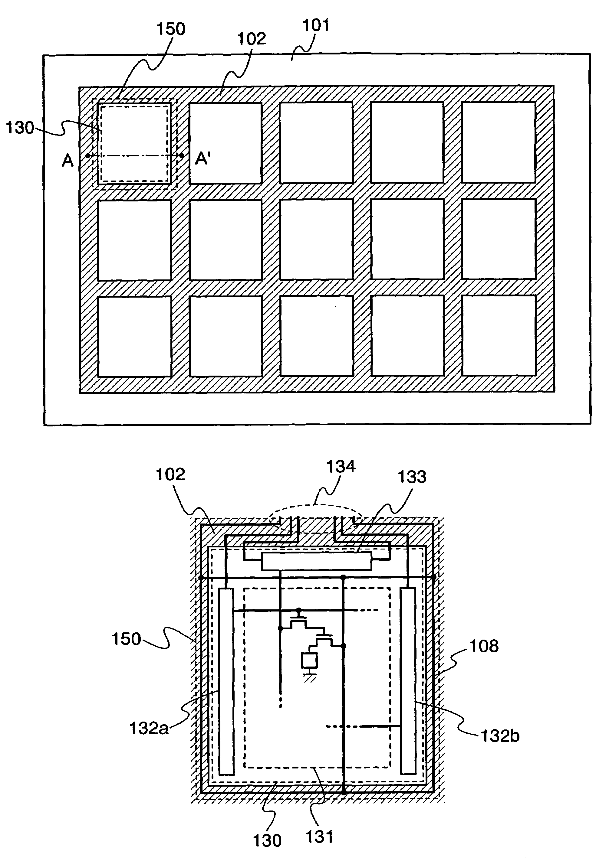
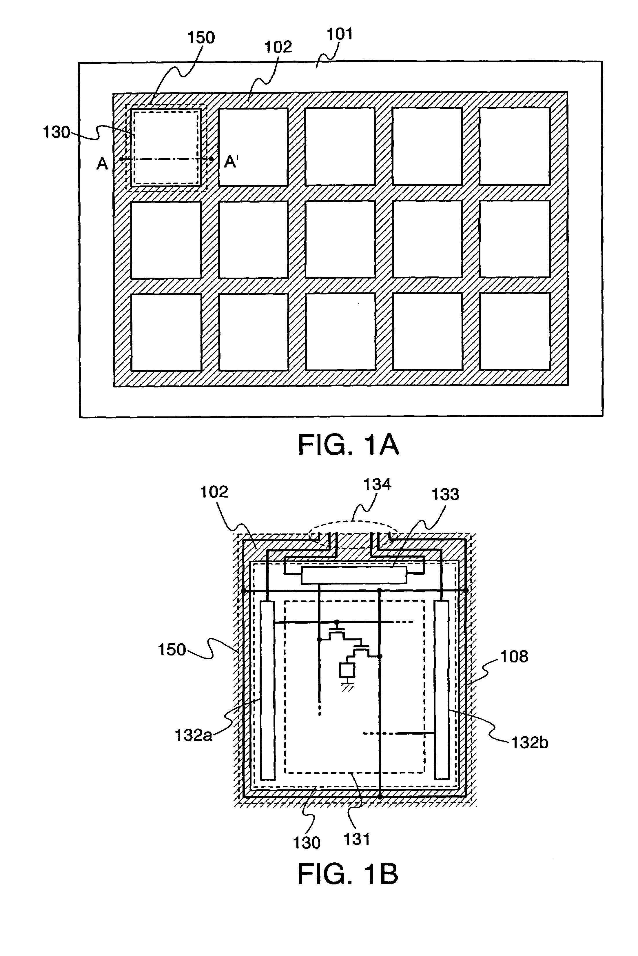
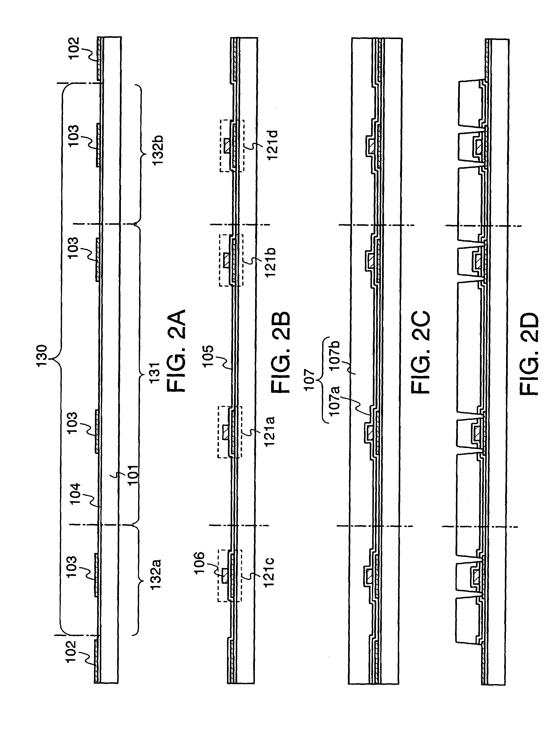
[0032]FIG. 1A is a top view explaining the method for manufacturing the light emitting devices of the invention, while FIGS. 2A to 2D and FIGS. 3A to 3C are cross sectional views explaining the method for manufacturing the light emitting device of the invention. FIG. 2A is a cross sectional view taken along a dashed line A–A′ of FIG. 1A.

[0033]As shown in FIG. 1A, a first grid-like semiconductor layer 102 extending in rows and columns is formed over a substrate 101. While forming the first grid-like semiconductor layer 102, plural second island-like semiconductor layers 103 are formed inside of regions 130 surrounded by the first grid-like semiconductor layer 102, as shown in FIG. 2A. Here, the secon...

embodiment mode 2

[Embodiment Mode 2]

[0059]The method for manufacturing the light emitting devices as described in Embodiment Mode 1 and another mode of the present invention will be described in the present embodiment mode with reference to FIGS. 4A to 4C and FIGS. 5A to 5C.

[0060]A first grid-like semiconductor layer 202 extending in rows and columns is formed over a substrate 201 as well as the first semiconductor layer 102 as shown in Embodiment Mode 1. While forming the first semiconductor layer 202, plural second island-like semiconductor layers 203 are formed inside of each region 230 surrounded by the first semiconductor layer 202 in the same manner as the second island-like semiconductor layers 103 as shown in Embodiment Mode 1. The second semiconductor layers 203 are formed to fabricate transistors. Through steps as described later, plural light emitting devices each of which is included in one region 230 surrounded by the first semiconductor layer 202 as a unit are formed over the substrate...

embodiment mode 3

[Embodiment Mode 3]

[0087]Light emitting devices manufactured according to the present invention as shown in Embodiment Modes 1 and 2 will be described in the present embodiment mode.

[0088]This embodiment mode will describe modes of the light emitting devices formed according to the present invention. Note that configurations of the light emitting devices according to the invention and substances of the light emitting devices are not limited to the present embodiment mode.

[0089]In the light emitting devices as shown in FIGS. 3C and 5C, the light emitting layer 112 that is a constituent element of the light emitting element 114 and the light emitting layer 213 that is a constituent element of the light emitting element 215 include plural layers, respectively. The plural layers are formed by combining layers made from substances selected from substances with excellent carrier transporting properties and excellent carrier injecting properties. The plural layers partly contain a substanc...


PUM


Abstract

An object of the invention is to provide a method for manufacturing a light emitting device capable of reducing deterioration of elements due to electrostatic charge caused in manufacturing the light emitting device. Another object of the invention is to provide a light emitting device in which defects due to the deterioration of elements caused by the electrostatic charge are reduced. The method for manufacturing the light emitting device includes a step of forming a top-gate type transistor for driving a light emitting element. In the step of forming the top-gate type transistor, when processing a semiconductor layer, a first grid-like semiconductor layer extending in rows and columns is formed over a substrate. The plurality of second island-like semiconductor layers are formed between the first semiconductor layer. The plurality of second island-like second semiconductor layers serve as an active layer of the transistor.

Description

BACKGROUND OF THE INVENTION[0001]1. Field of the Invention[0002]The present invention relates to a light emitting device manufactured by using a large size substrate and a method for manufacturing thereof.[0003]2. Description of the Related Art[0004]A light emitting device utilizing light emission of an electroluminescent element (a light emitting element) has been attracting attention as a display device with wide viewing angle and low power consumption. In recent years, development for the purpose of mass-production of such the light emitting devices has been carried out.[0005]One of the problems in the mass-production of the light emitting devices is the development of a technique for manufacturing the light emitting devices by using a large size substrate. By using the large size substrate, a large size television and the like can be manufactured. In addition, small light emitting devices that are mounted on small electronic appliances such as cellular phones can be mass-produce...

Claims


Application Information

Patent Timeline
Patent Type & Authority Patents(United States)
IPC IPC(8): H01L21/00H01L21/84H01L27/32H01L29/04H01L51/52H05B33/02H05B33/10H05B33/12H05B44/00
CPCH01L27/3244H01L51/5246H01L2251/566H01L27/3276H10K59/12H10K59/131H10K50/8426H10K71/851
Inventor MURAKAMI, SATOSHISAKAKURA, MASAYUKI
Owner SEMICON ENERGY LAB CO LTD
Why Eureka
Try Eureka