Spatial filter for sample inspection system

a sampling inspection and spatial filter technology, applied in the field of spatial filtering in optical sampling inspection systems, can solve the problems of difficult to distinguish signals scattered from defects, wafer surface defects, scattering noise, etc., and achieve the effects of enhancing snr, improving sensitivity, and suppressing nois

Active Publication Date: 2007-02-27
KLA TENCOR TECH CORP
View PDF7 Cites 30 Cited by
  • Summary
  • Abstract
  • Description
  • Claims
  • Application Information

AI Technical Summary

Benefits of technology

[0030]A sample inspection system of the type depicted in FIG. 1 can have a very large collection angle in dark field. A large collection angle makes such a system very sensitive for smooth wafers, such as prime silicon wafers. However, this large collection angle becomes a weakness when scanning a rough surface, such as the backside of a single side polished (SSP) wafer or other rough surface. The signal to noise ratio (SNR) for a sample inspection system determines its sensitivity. However, because of the heavy noise of a rough surface, suppressing the noise becomes the key factor for gaining a better sensitivity. Generally, one enhances SNR by increasing the signal and / or suppressing noise.
[0031]The scattered radiation 55 is scattered in a direction having an azimuthal component and elevation component with respect to the symmetry axis z. The inventor has analyzed the scatter distribution for both signal and noise from rough surfaces (e.g., the backside of SSP wafers). The analysis shows that for very rough wafers, i.e., wafers with surface features characterized by a relatively high spatial frequency compared to the frequency of incident radiation, most of the noise (i.e., radiation scattered from other surface features) is forward scattered, while most of the signal from small defects (i.e., radiation scattered from small defects), which actually determines the system sensitivity, is backscattered. Note that for very small defects, e.g., less than about 80 nm, most of the scattered radiation 55 is backscattered. An example of a worst-case noise distribution in the vertical plane is indicated schematically at 55 in FIG. 1. Nearly all of the backscattered noise is backscattered at angles less than about 45° with respect to the surface normal (symmetry axis z). Backscattered noise can be a significant problem if the noise is above a threshold of the detector 80. Based on the surface scatter distribution in 3-D, the inventor has developed a new spatial filter. This type of filter has been tested on backside inspection module (BSIM) systems with many different types of SSP wafers from different venders. The test results indicate that the new spatial filter significantly enhances BSIM sensitivity.

Problems solved by technology

The pattern of scattering can reveal defects in the wafer surface.
However, the extreme roughness of the surfaces involved often produces scattering noise that can be difficult to distinguish from signal scattered from defects.

Method used


Image

  • Spatial filter for sample inspection system
  • Spatial filter for sample inspection system
  • Spatial filter for sample inspection system

Examples


Embodiment Construction

[0023]Although the following detailed description contains many specific details for the purposes of illustration, anyone of ordinary skill in the art will appreciate that many variations and alterations to the following details are within the scope of the invention. Accordingly, the exemplary embodiments of the invention described below are set forth without any loss of generality to, and without imposing limitations upon, the claimed invention.

Sample Inspection Systems

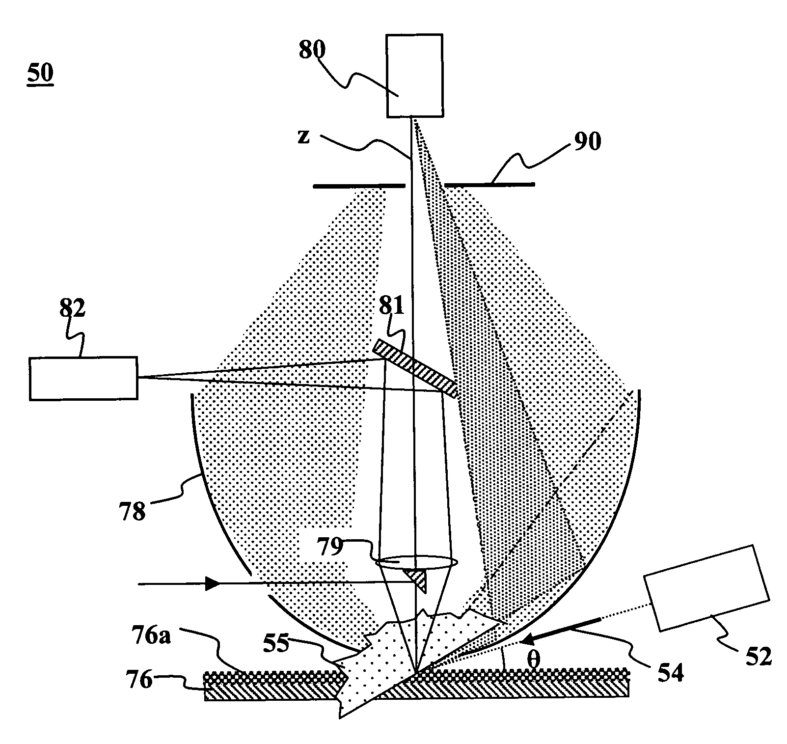
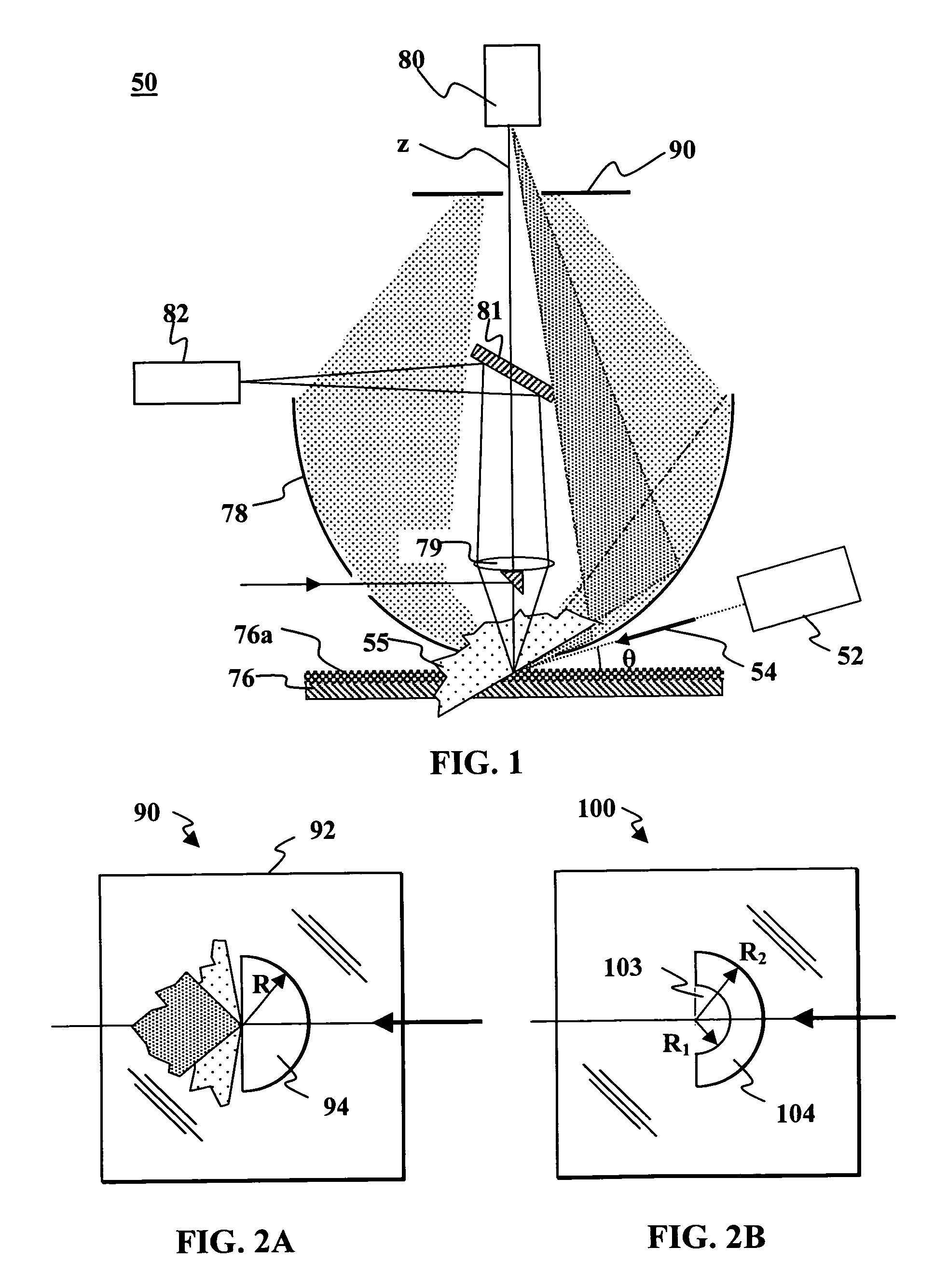
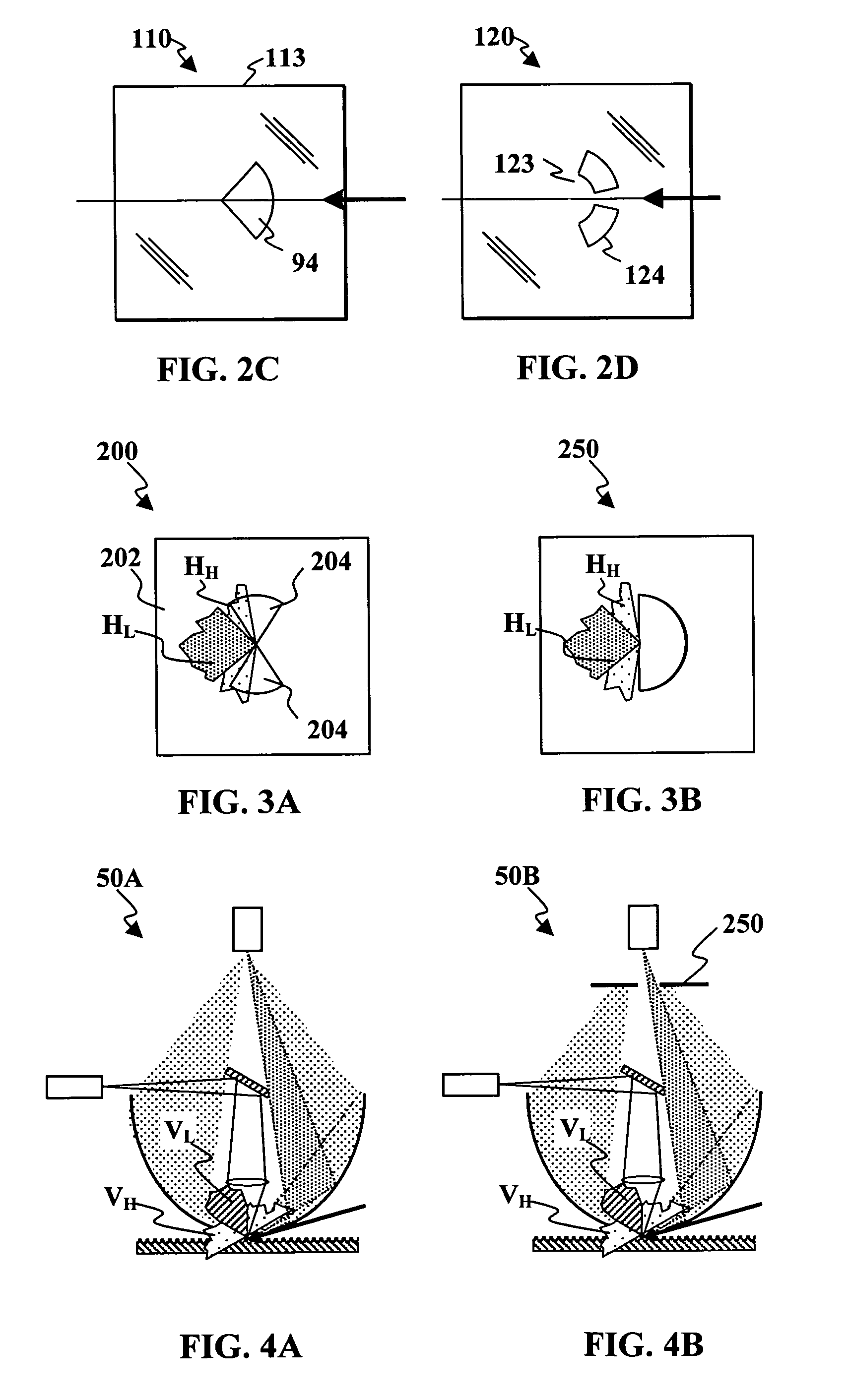
[0024]According to embodiments of the present invention, spatial filtering can improve the signal to noise ration of a sample inspection system of the type having a detector and collection optics that receive radiation scattered from a point on a sample surface and direct the scattered radiation toward the detector. The spatial filtering screens the detector from substantially all of the forward-scattered radiation and from back-scattered radiation that is scattered in at an elevation angle less than about 45° with r...


PUM

PropertyMeasurementUnit
elevation angleaaaaaaaaaa
elevation anglesaaaaaaaaaa

Abstract

Spatial filtering is disclosed that improves the signal to noise ration of a sample inspection system of the type having a detector and collection optics that receive radiation scattered from a point on a sample surface and direct the scattered radiation toward the detector. The spatial filtering may screen the detector from substantially all of the forward-scattered radiation from back-scattered radiation that is scattered in a at an elevation angle less than about 45° with respect to a normal to the surface. Forward scattered noise is screened from the detector while backscattered signal reaches the detector. Programmable spatial filters may be used to selectively block scattered noise due to surface roughness while transmitting scattered signal due to surface defects.

Description

FIELD OF THE INVENTION[0001]This invention generally relates to optical sample inspection systems and more specifically to spatial filtering in optical sample inspection systems.BACKGROUND OF THE INVENTION[0002]Systems for inspecting semiconductor wafers or bare wafers have been proposed. See for example, U.S. Pat. No. 6,201,601. Systems such as those described in the above-referenced patent are useful for many applications, including the inspection of bare or unpatterned semiconductor wafers. Such systems typically scatter a laser beam from the wafer surface and collect the scattered radiation at a detector. The pattern of scattering can reveal defects in the wafer surface.[0003]It is often desirable to use such sample inspection tools to inspect not only bare or unpatterned wafers but also rough surfaces, such as those found on the backside of a single-side polished (SSP) wafer. However, the extreme roughness of the surfaces involved often produces scattering noise that can be dif...

Claims


Application Information

Patent Timeline
Patent Type & Authority Patents(United States)
IPC IPC(8): G01N21/00G01B11/30
CPCG01N21/9501G01N21/8806
Inventor LI, BO
Owner KLA TENCOR TECH CORP
Why Eureka
Try Eureka