Mover device and semiconductor manufacturing apparatus and method

a semiconductor manufacturing and moving device technology, applied in the direction of motor/generator/converter stopper, dynamo-electric converter control, instruments, etc., can solve the problems of increased driving reaction force, unfavorable impact and vibration, noise, etc., and achieve the effect of reducing the load on the moving force generating unit and facilitating the reverse of the processing bas

Inactive Publication Date: 2007-03-06
SEN CORP AN SHI & AXCELIS
View PDF13 Cites 15 Cited by
  • Summary
  • Abstract
  • Description
  • Claims
  • Application Information

AI Technical Summary

Benefits of technology

[0010]A more specific object of the present invention is to provide a mover device and a semiconductor manufacturing apparatus in which a processing base can reciprocate at a high speed without undesirable impact, vibration, and noise.
[0167]By this method, the reaction force caused by the acceleration or deceleration movement of the processing base can be completely absorbed. Also, cogging force generation can be prevented. Accordingly, the auxiliary driving unit can smoothly move the processing base and the movable base with high precision. Furthermore, the moving velocity of the processing base can be adjusted to a predetermined uniform velocity promptly, and the processing base can be stopped promptly. Accordingly, the uniform velocity region can be widened. When the processing base and the movable base change moving states at the same time (for example, from an accelerating state to a uniform velocity moving state), the processing base and the movable base can interact with each other so as to prevent a positional deviation.

Problems solved by technology

The driving reaction forces cause impact and vibration that are undesirable for movements of the processing base during operations.
This also causes greater driving reaction forces.
As a result, conventional methods of preventing driving reaction force generation cannot effectively restrict undesirable impact, vibration, and noise in a mover device.

Method used


Image

  • Mover device and semiconductor manufacturing apparatus and method
  • Mover device and semiconductor manufacturing apparatus and method
  • Mover device and semiconductor manufacturing apparatus and method

Examples


first embodiment

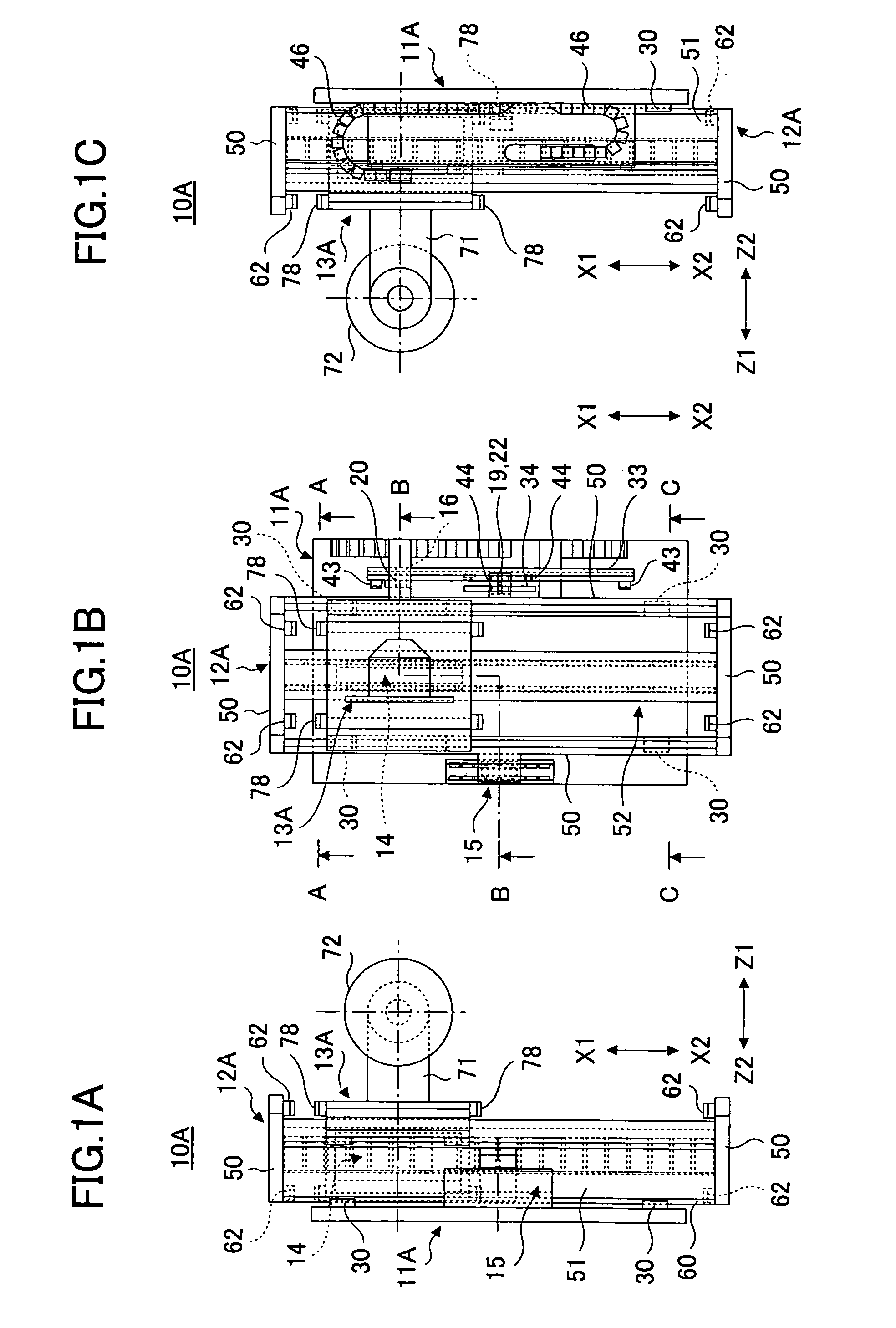
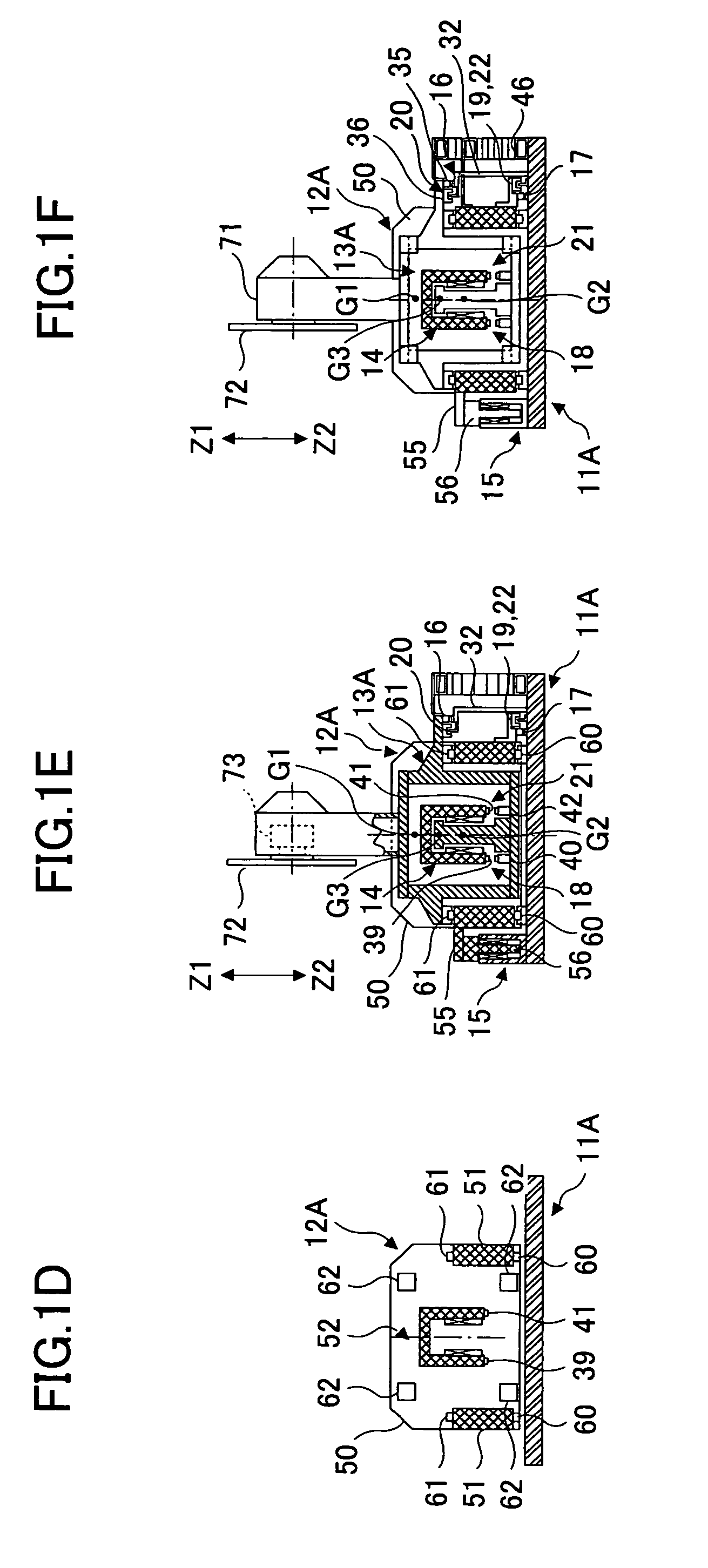
[0212]FIGS. 1A through 4C illustrate the hardware structure of a mover device 10A in accordance with the present invention. FIGS. 1A through 1F illustrate the entire structure of the mover device 10A. FIGS. 2A through 2C illustrate a fixed base 11A. FIGS. 3A through 3C illustrate a movable base 12A. FIGS. 4A through 4C illustrate a processing base 13A.

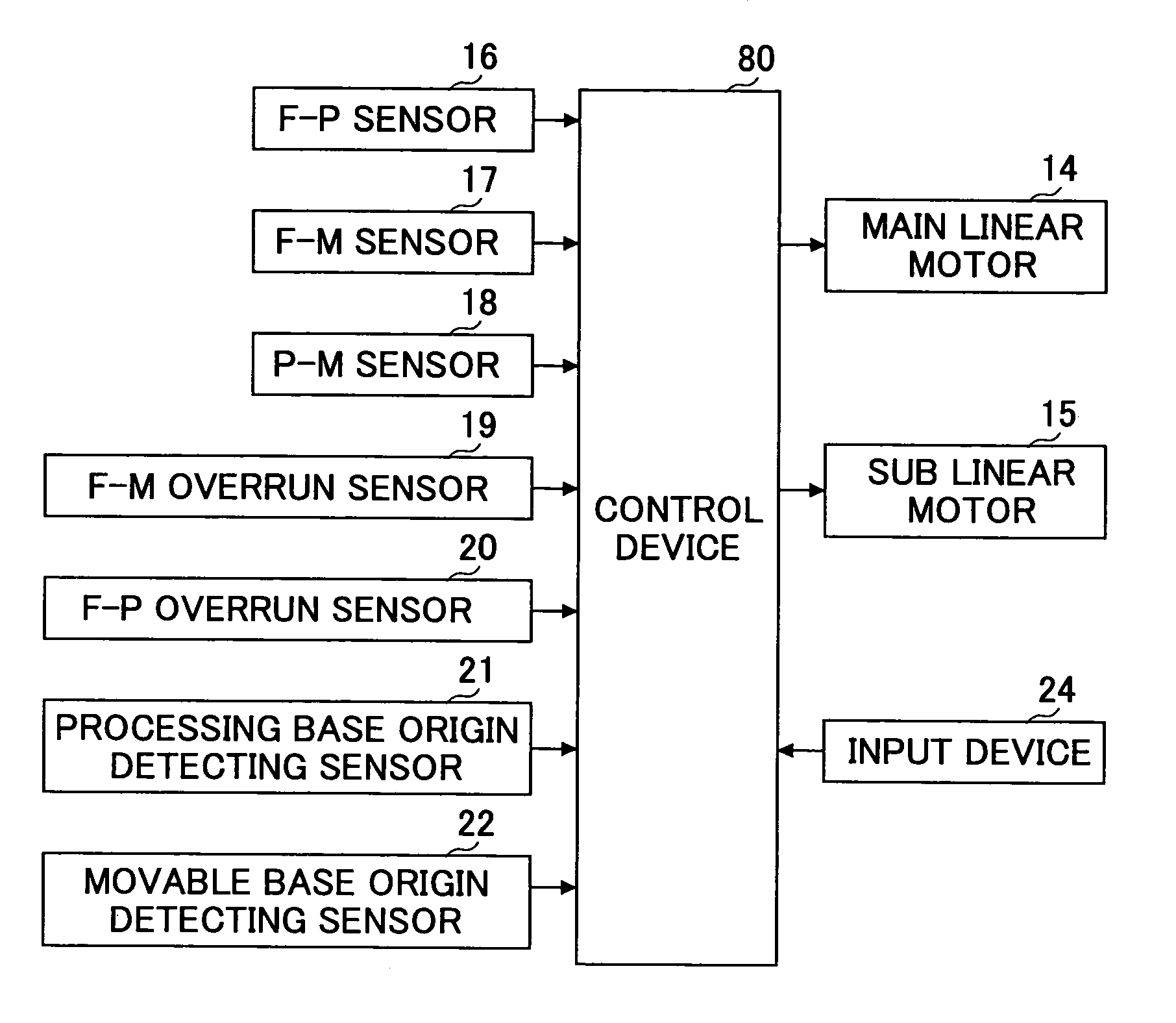
[0213]As shown in FIGS. 1A through 1F, the mover device 10A includes the fixed base 11A, the movable base 12A, the processing base 13A, a main linear motor 14, and a sub linear motor 15. The mover device 10A linearly moves the processing base 13A in a reciprocation manner in the directions of the arrows X1 and X2 shown in the drawings. This is carried out in accordance with a control operation performed by a later described control device 80 (see FIG. 6).

[0214]The fixed base 11A will be first described. As shown in FIGS. 1A through 1F and FIGS. 2A through 2C, the fixed base 11A has a linear guide block 30 in the vicinity of each of the...

second embodiment

[0408]FIGS. 18A through 18F illustrate the mover device 10B in accordance with the

[0409]The mover device 10A of the first embodiment has only one moving force generator, which is the main linear motor 14. The mover device 10B of this embodiment, on the other hand, has two main linear motors 14A and 14B. With the two main linear motors 14A and 14B that function as moving force generators, the acceleration and the deceleration of the processing base 13A can be increased. Also, even if the weight of the processing base 13A increases as the parts of the processing base 13A become larger to accommodate larger wafers, the processing base 13A of this embodiment can stably reciprocate with precision.

third embodiment

[0410]FIGS. 19A through 19F illustrate the mover device 10C in accordance with the

[0411]In the mover device 10A of the first embodiment, the wafer attaching face of the platen 72 is perpendicular to the fixed base 11A. In the mover device 10C of this embodiment, on the other hand, the wafer attaching face of the platen 72 provided on the processing base 13A is in parallel with the fixed base 11A. With this structure, each wafer can be processed in a laid state.

[0412]FIGS. 20A through 20C illustrate the mover device 10D in accordance with the fourth embodiment. The mover device 10A in accordance with the first embodiment has the sub linear motor 15. On the other hand, the mover device 10D of this embodiment does not include the sub linear motor 15.

[0413]Since a driving means for moving the movable base 12A with respect to a fixed base 11B does not exist in this embodiment, the movable base 12A is moved by the repulsion force generated from the processing base 13A moving with respect ...


PUM


Abstract

A mover device and an ion implanter apparatus having a processing base that reciprocates at a high speed without undesirable noise and vibration are provided. The mover device includes: a fixed base; a movable base that is linearly movable with respect to the fixed base; a processing base that is linearly movable with respect to the movable base; a main linear motor that generates a moving force to move the processing base with respect to the movable base, thereby moving the processing base with respect to the fixed base; and a velocity control unit that controls the moving velocity of the processing base with respect to the fixed base. In this mover device, the movable base is moved by virtue of a reaction force caused by the moving force to move the processing base.

Description

BACKGROUND OF THE INVENTION[0001]The present invention generally relates to mover devices and semiconductor manufacturing apparatuses, and, more particularly, to a mover device and a semiconductor manufacturing apparatus in which a processing base reciprocates at a high speed.[0002]In semiconductor manufacturing apparatuses and liquid crystal manufacturing apparatuses, a large number of production procedures are normally carried out for each substrate (semiconductor substrate).[0003]More specifically, the following processes are carried out: a sputtering process for physically forming a thin film on a substrate; a CVD sputtering process for forming a thin film on a substrate through chemical vapor deposition; a lithography process for processing the shape of a thin film formed on a substrate; an impurity adding process for adding impurities to a film formed on a substrate; an etching process for etching a thin film formed on a substrate; an electronic beam process for performing min...

Claims


Application Information

Patent Timeline
Patent Type & Authority Patents(United States)
IPC IPC(8): H02P1/00H01L21/68H01L21/677
CPCH01L21/67709Y10T74/15
Inventor OKADA, KEIJIHIDAKA, YOSHITOMOSUGITANI, MICHIROMURAKAMI, JUNICHISATO, FUMIAKITSUKIHARA, MITSUKUNIHIROKAWA, SUGURUSHINOZUKA, MASAMITSU
Owner SEN CORP AN SHI & AXCELIS
Why Eureka
Try Eureka