Method and apparatus for clockless analog-to-digital conversion and peak detection

a clockless analog-to-digital and peak detection technology, applied in the field of analog-to-digital conversion, can solve the problems of inability to integrate efficient circuits for the processing of shaped pulses, inability to discriminate multiple windows, and inability to achieve multiple windows at the same time, so as to minimize the processing time of shaped pulses and reduce the loss of data. , the effect of power

Active Publication Date: 2007-03-06
BROOKHAVEN SCI ASSOCS
View PDF14 Cites 17 Cited by
  • Summary
  • Abstract
  • Description
  • Claims
  • Application Information

AI Technical Summary

Benefits of technology

[0030]As a result, the present invention provides peak detection and analog-to-digital conversion of shaped analog pulses caused by an ionizing event in a radiation detection system without requiring a clock signal and using very little power. In addition, since analog-to-digital conversion occurs during a rising edge of the shaped pulse and conversion is complete when the peak occurs, the present invention advantageously minimizes the processing time of the shaped pulse and, as a consequence, the loss of data. These and other objects, features, and advantages of this invention will become apparent from the following detailed description of illustrative embodiments thereof, which is to be read in connection with the accompanying drawings.

Problems solved by technology

The integration of efficient circuits for the processing of the shaped pulses represents a challenge, especially when the number m of discrete levels exceeds a few units.
The main disadvantage of this approach appears when the number of windows exceeds a few units.
As the number of discrete levels m increases above a few units, the multiple-windows discrimination approach becomes impractical and the analog peak detection with peak digitization method shown in FIG. 4 is typically adopted.
The primary disadvantage of this approach is the amount of power required by the peak detection and the on-chip analog-to-digital conversion per channel.
There are a very large number of ADC architectures available, but only very few configurations may actually satisfy the stringent power requirements of any particular application.
Some mixed solutions make use of multiplexers and arbitration logic to share one ADC among several channels to save power, but this saving is at the expense of substantially greater complexity.
Another disadvantage of this approach is the need for an external or internally generated clock signal, which is required by the ADC 24 in order to provide the conversion.
The clock signal can easily interfere with the low-noise analog front-end circuitry with consequent degradation of the resolution.
One last disadvantage is represented by the total amount of time required for detecting and converting the peak, which is equal to the sum of the peak detection time plus the conversion time.
Depending on the speed of the ADC and the rate of the application, this time can become long enough to cause loss of data.
The main disadvantage of this approach is the power required to provide fast on-chip analog-to-digital conversion per channel.
In addition, the disadvantage of requiring an external or internally generated clock applies in this method.

Method used


Image

  • Method and apparatus for clockless analog-to-digital conversion and peak detection
  • Method and apparatus for clockless analog-to-digital conversion and peak detection
  • Method and apparatus for clockless analog-to-digital conversion and peak detection

Examples


Embodiment Construction

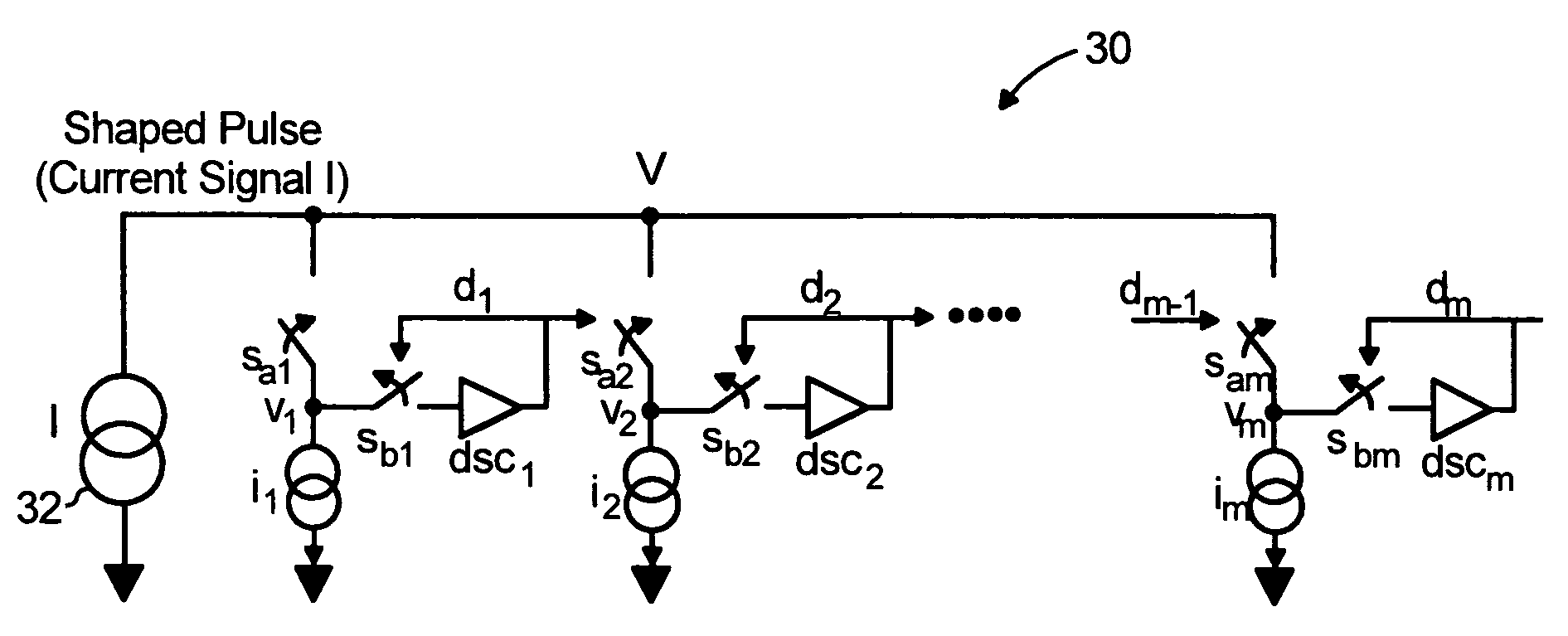
[0043]A clockless analog-to-digital converter and peak detector circuit 30 formed in accordance with the present invention and shown in the schematic diagram of FIG. 6 provides peak detection and analog-to-digital conversion of a shaped pulse, which represents an ionizing event, from a front-end portion of a radiation detection system. The circuit 30 exhibits low power dissipation, requires little power, and does not need a clock signal. The circuit 30 is preferably operated in current-mode, which means that it operates on the basis of current rather than voltage. If the shaped pulse is a voltage signal, a voltage-to-current converter is preferably used to convert the signal before processing by this circuit. A representative voltage-to current conversion circuit 33 is shown in FIG. 12, in which the voltage signal is applied at terminal A and the current signal is obtained from terminal B. The circuit 33 preferably includes four (4) transistors Mr1, Mr2, M1, M2, a resistor R1, and a...


PUM


Abstract

An apparatus and method for analog-to-digital conversion and peak detection includes at least one stage, which includes a first switch, second switch, current source or capacitor, and discriminator. The discriminator changes state in response to a current or charge associated with the input signal exceeding a threshold, thereby indicating whether the current or charge associated with the input signal is greater than the threshold. The input signal includes a peak or a charge, and the converter includes a peak or charge detect mode in which a state of the switch is retained in response to a decrease in the current or charge associated with the input signal. The state of the switch represents at least a portion of a value of the peak or of the charge.

Description

[0001]This invention was made with support from the U.S. Government under Contract No. DE-AC0298CH10886 by the U.S. Department of Energy. The U.S. Government has certain rights in the invention.BACKGROUND OF THE INVENTION[0002]1. Field of the Invention[0003]The present invention relates to analog-to-digital conversion, and more particularly to performing analog-to-digital conversion without requiring a clock signal.[0004]2. Description of the Prior Art[0005]The front-end portion of a radiation detection system, as shown in FIG. 1, typically includes a sensor 12 (e.g. pixel), which provides the conversion of the ionizing radiation into a charge Q, a charge amplifier 14, which provides conversion of the charge Q into a voltage V, and a filter or shaping amplifier 16, which shapes the signal into a pulse P shown in FIG. 2 with an amplitude proportional to the charge Q. The sensor 12 has pixel capacitance Cp, the charge amplifier 14 has input capacitance Ci and feedback capacitance Cf, ...

Claims


Application Information

Patent Timeline
Patent Type & Authority Patents(United States)
IPC IPC(8): H03M1/12
CPCG01R19/04H03M1/42G01T1/17G01R29/24
Inventor DEGERONIMO, GIANLUIGI
Owner BROOKHAVEN SCI ASSOCS
Why Eureka
Try Eureka