

Apparatus and method for inspecting defects
a technology of defect inspection and defect detection, applied in the direction of semiconductor/solid-state device testing/measurement, instruments, image data processing, etc., can solve the problems of short circuit, insulation failure, short circuit of wiring formed on it, etc., and achieve high efficiency, high reliability, and high reliability
- Summary
- Abstract
- Description
- Claims
- Application Information
AI Technical Summary
Benefits of technology
Problems solved by technology
Method used
Image

Examples
Embodiment Construction
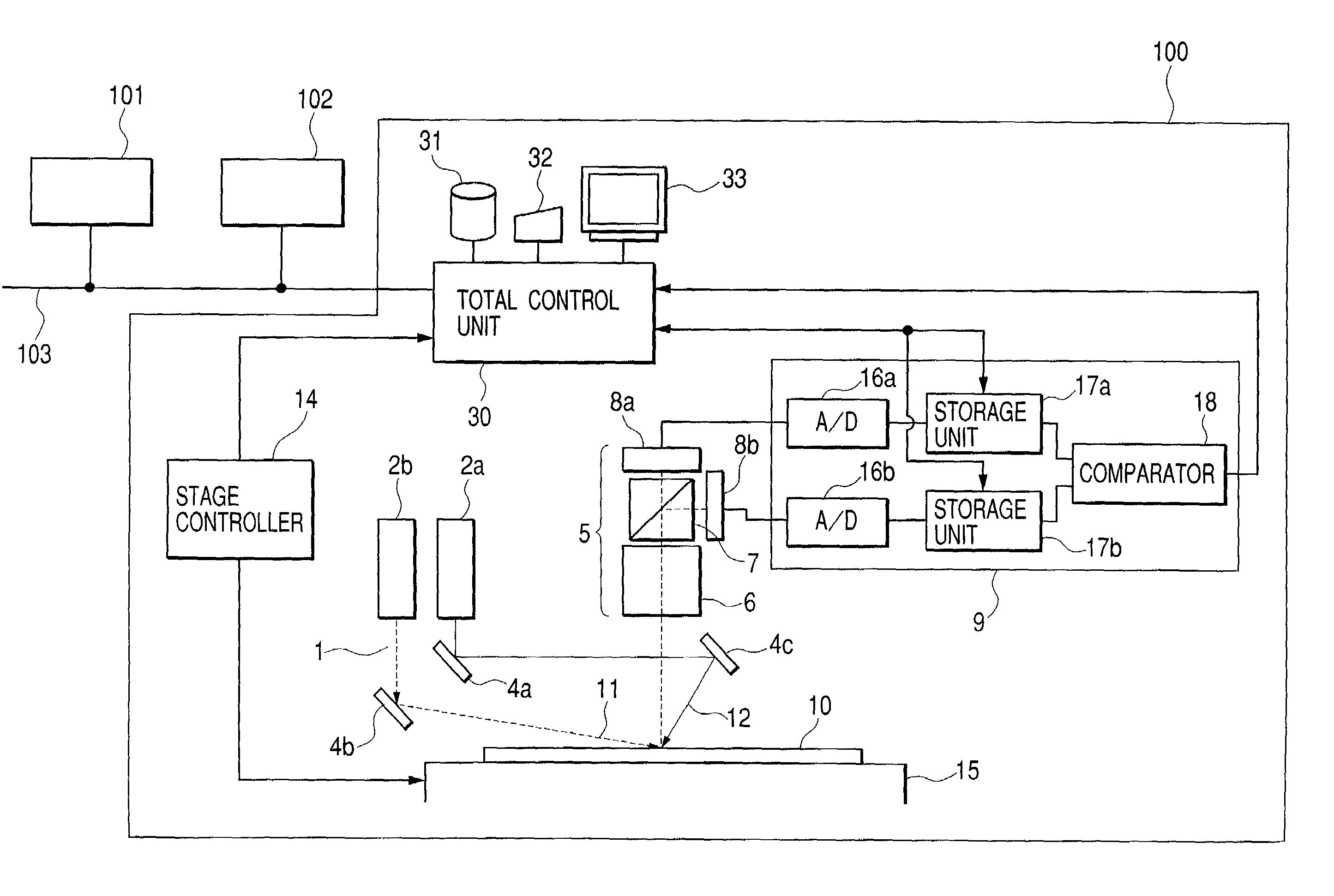
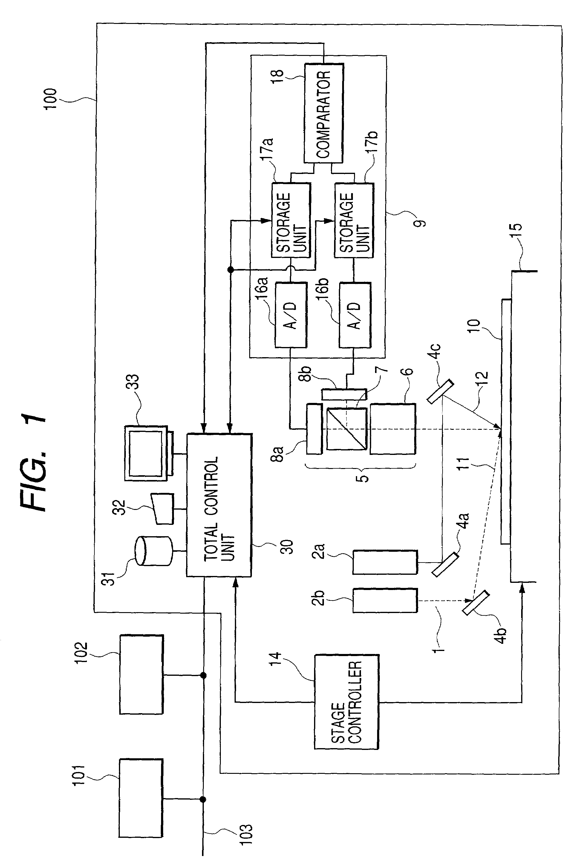
[0078]Embodiments of a defect-inspecting apparatus and method according to the present invention, which are used in a semiconductor production process or a magnetic head production process, and which aim to operate a planarization fabrication process with stability, will be described with reference to drawings as below.
[0079]In the first place, a first embodiment of the defect-inspecting apparatus and its method according to the present invention will be described. As shown in FIG. 1, the present invention relates to a defect-inspecting apparatus 100 that performs sampling inspection or hundred-percent inspection of products in the middle of a semiconductor production process. As regards a semiconductor production line, a process-control computer 101 manages production conditions, for example, through a network 103, or for each individual production equipment (not illustrated). In the middle of the process, a semiconductor is inspected using a foreign-material inspecting apparatus, ...
PUM
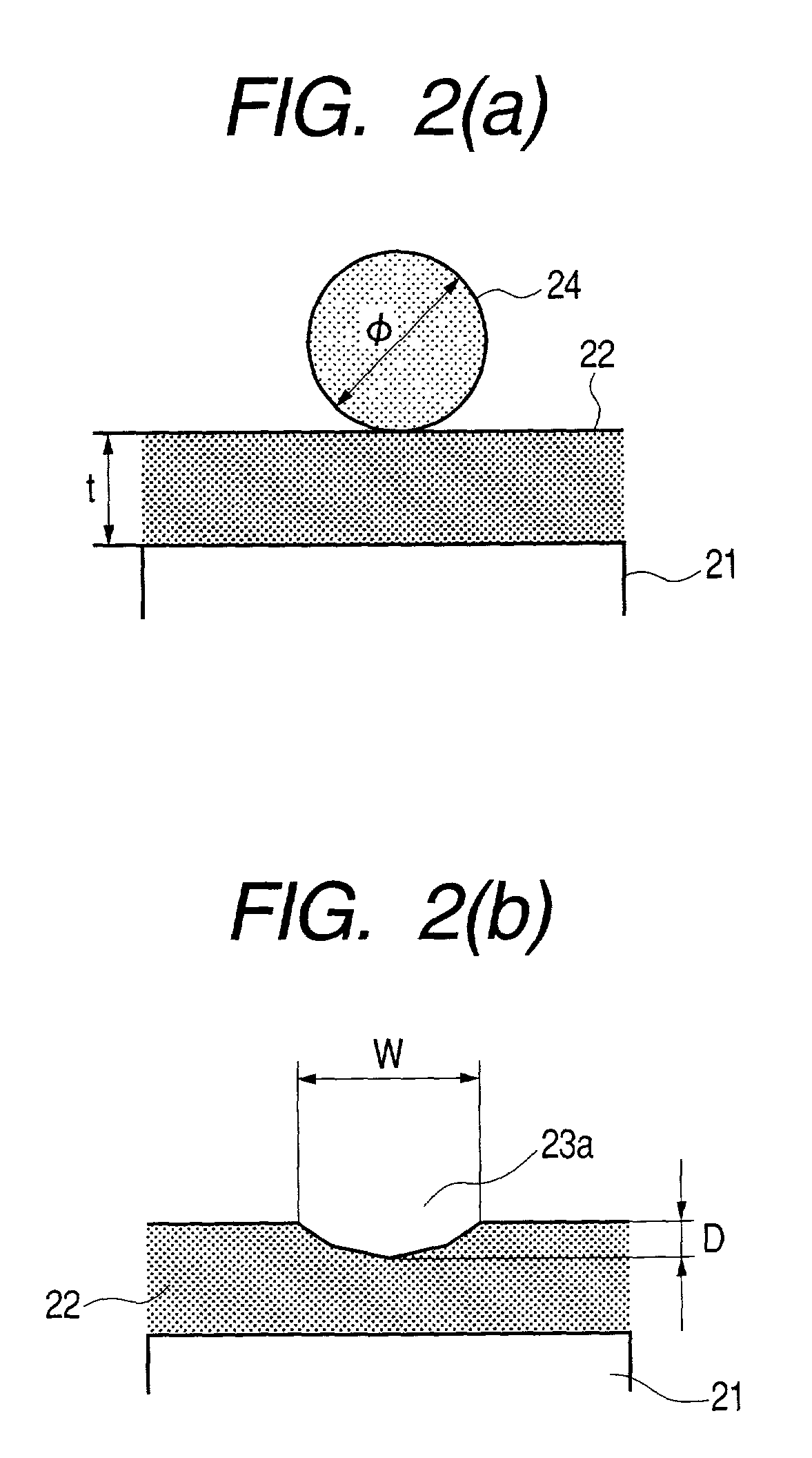
| Property | Measurement | Unit |
|---|---|---|
| elevation angle | aaaaa | aaaaa |
| depth | aaaaa | aaaaa |
| width | aaaaa | aaaaa |
Abstract
Description
Claims
Application Information