

Elimination of RDL using tape base flip chip on flex for die stacking
a flip chip and flex technology, applied in the direction of solid-state devices, basic electric elements, semiconductor devices, etc., can solve the problems of high cost and process difficulties, damage to the active surface, and the possibility of wafer bumping of bond pads, so as to improve interconnection and reduce the total assembly height
- Summary
- Abstract
- Description
- Claims
- Application Information
AI Technical Summary
Benefits of technology
Problems solved by technology
Method used
Image

Examples
Embodiment Construction
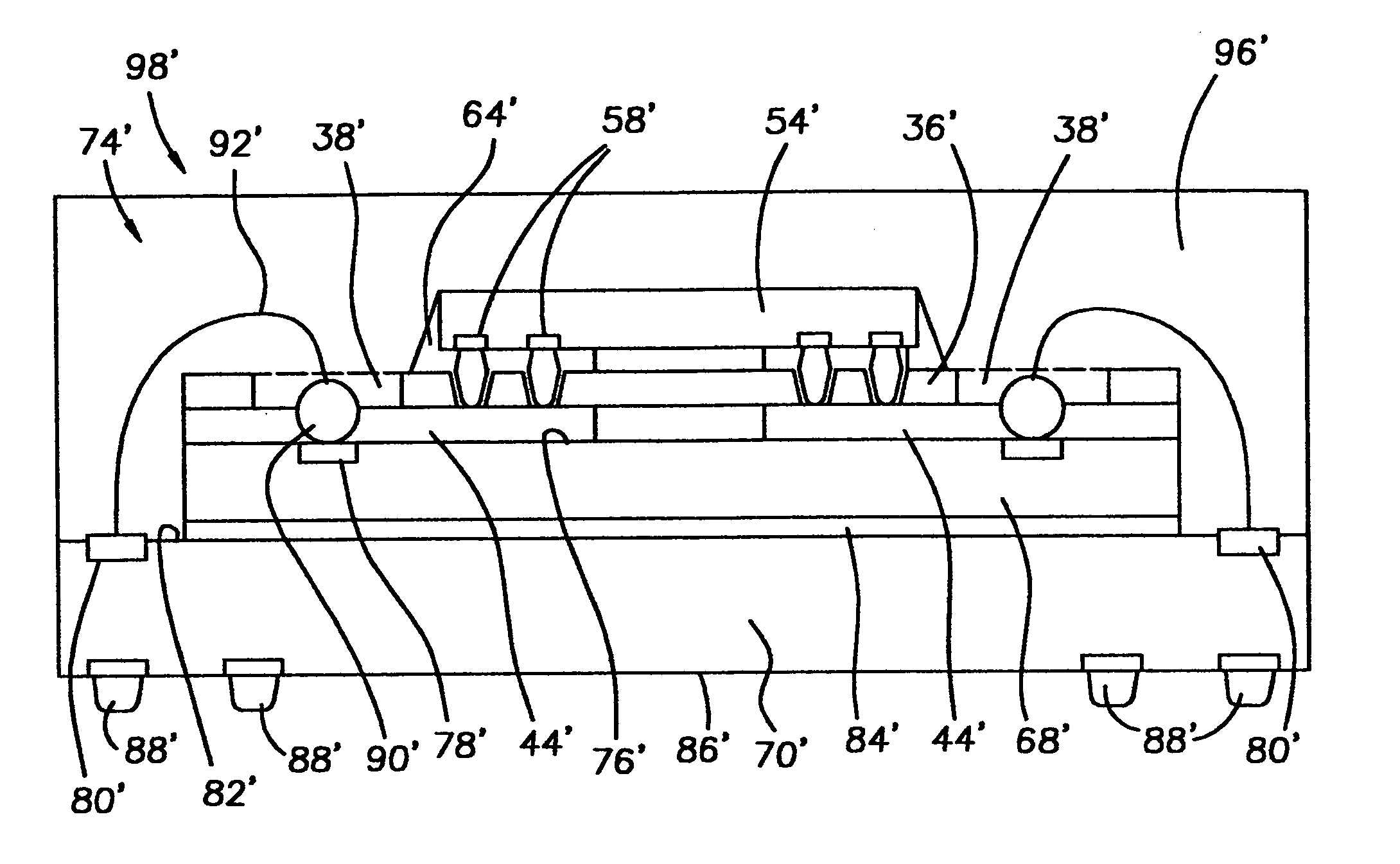
[0029]The invention will be described generally with reference to the drawings for the purpose of illustrating embodiments only and not for purposes of limiting the same. The figures illustrate processing steps for use in fabricating semiconductor devices in accordance with the present invention. It should be readily apparent that the processing steps are only a portion of the entire fabrication process.
[0030]The invention provides a flexible film interposer for stacking a tape base flip chip onto a second (bottom) die. Recesses are fabricated in the flexible film interposer for the first level interconnect using conventional die mount equipment. The flexible film interposer includes features to interconnect to the second die without the need for an RDL on the second die.
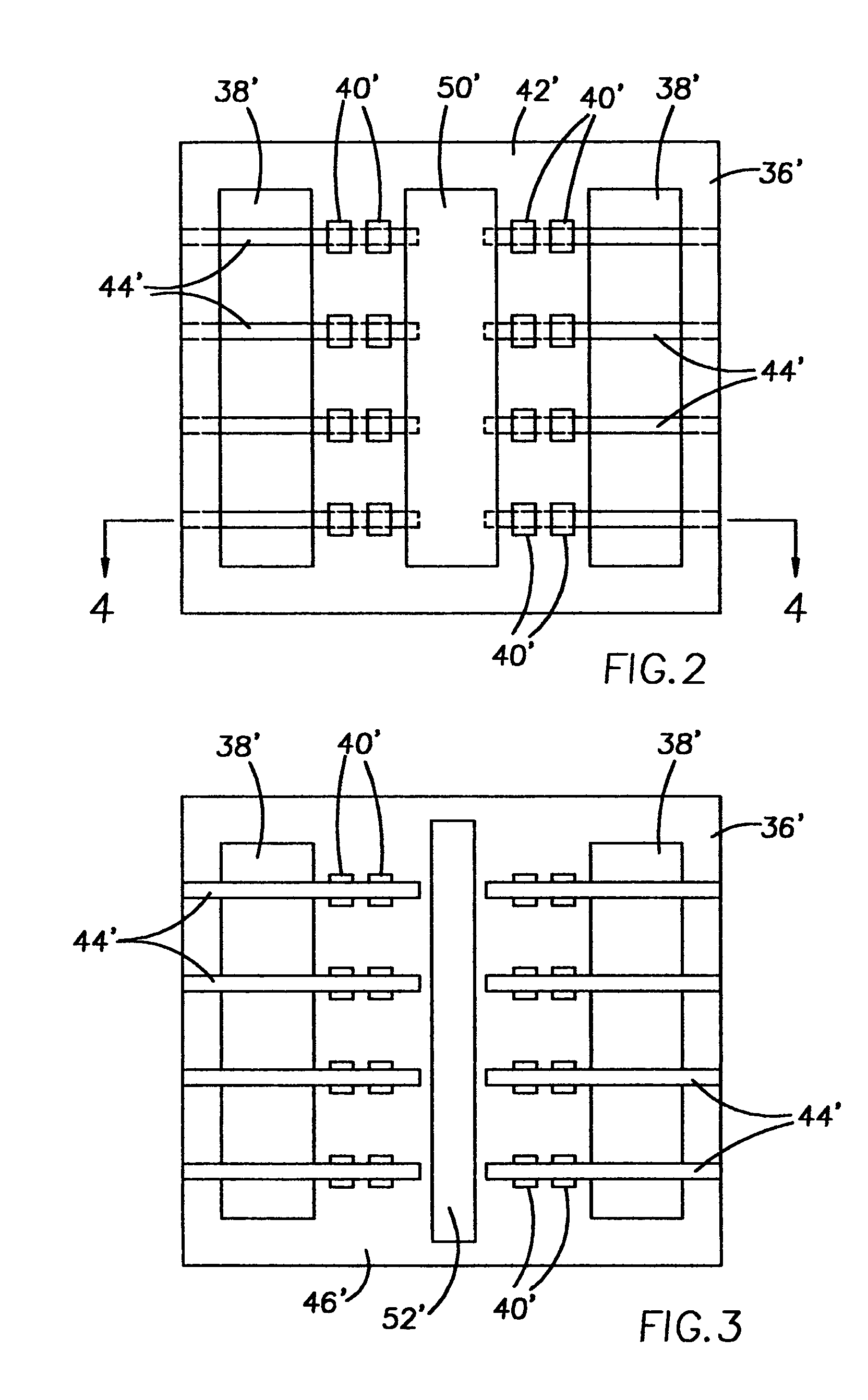
[0031]Referring to FIGS. 2–4, an embodiment of a flexible film interposer 36′ according to the invention is depicted in a simplified top plan view. The flexible film interposer 36′ can be formed from known insulatin...
PUM
| Property | Measurement | Unit |
|---|---|---|
| thickness | aaaaa | aaaaa |
| thicknesses | aaaaa | aaaaa |
| thicknesses | aaaaa | aaaaa |
Abstract
Description
Claims
Application Information