Control circuit and control method for DC-DC converter

Active Publication Date: 2007-03-20
CYPRESS SEMICON CORP
View PDF3 Cites 27 Cited by
  • Summary
  • Abstract
  • Description
  • Claims
  • Application Information

AI Technical Summary

Benefits of technology

[0014]First, a delay time in the current switching period is thus determined in accordance with a phase difference between a timing signal and a clock signal in a period before the current switching period. Accordingly, a phase difference between a timing signal and a clock signal generated in the current switching period does not have an influence on the delay time in the current switching period. And then, an inductor current value when the second state in the current switching period ends is made substantially equal to an average value of an inductor current value when the second state in the previous switching period ends. That is, a disturbance of an inductor current generated by a load fluctuation in the current switching period can be prevented from transmitt

Problems solved by technology

Thereupon, a problem is caused that a switching frequency of the transistor FET1 fluctuates depending on the input voltage Vin.
T

Method used


Image

  • Control circuit and control method for DC-DC converter
  • Control circuit and control method for DC-DC converter
  • Control circuit and control method for DC-DC converter

Examples


first embodiment

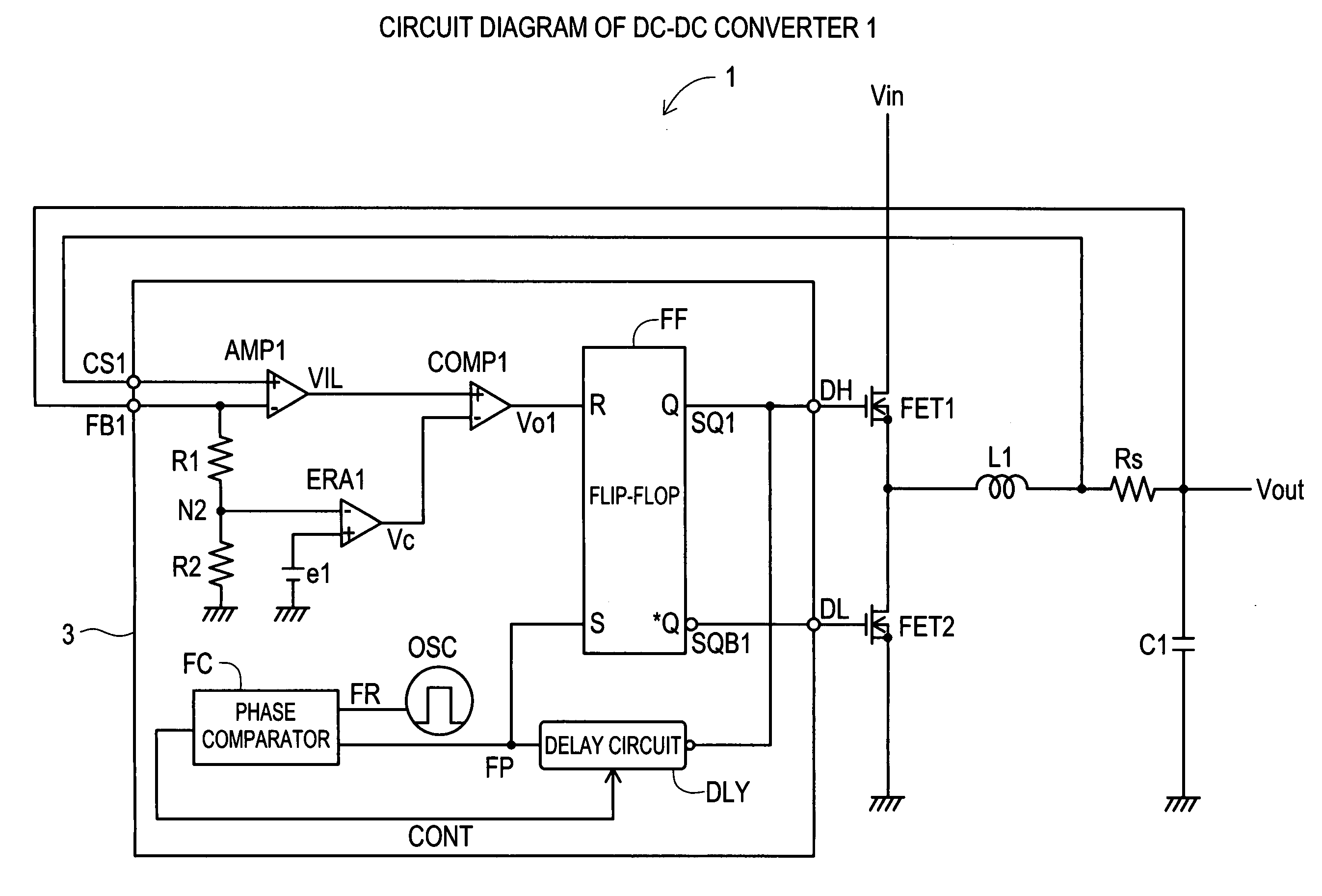
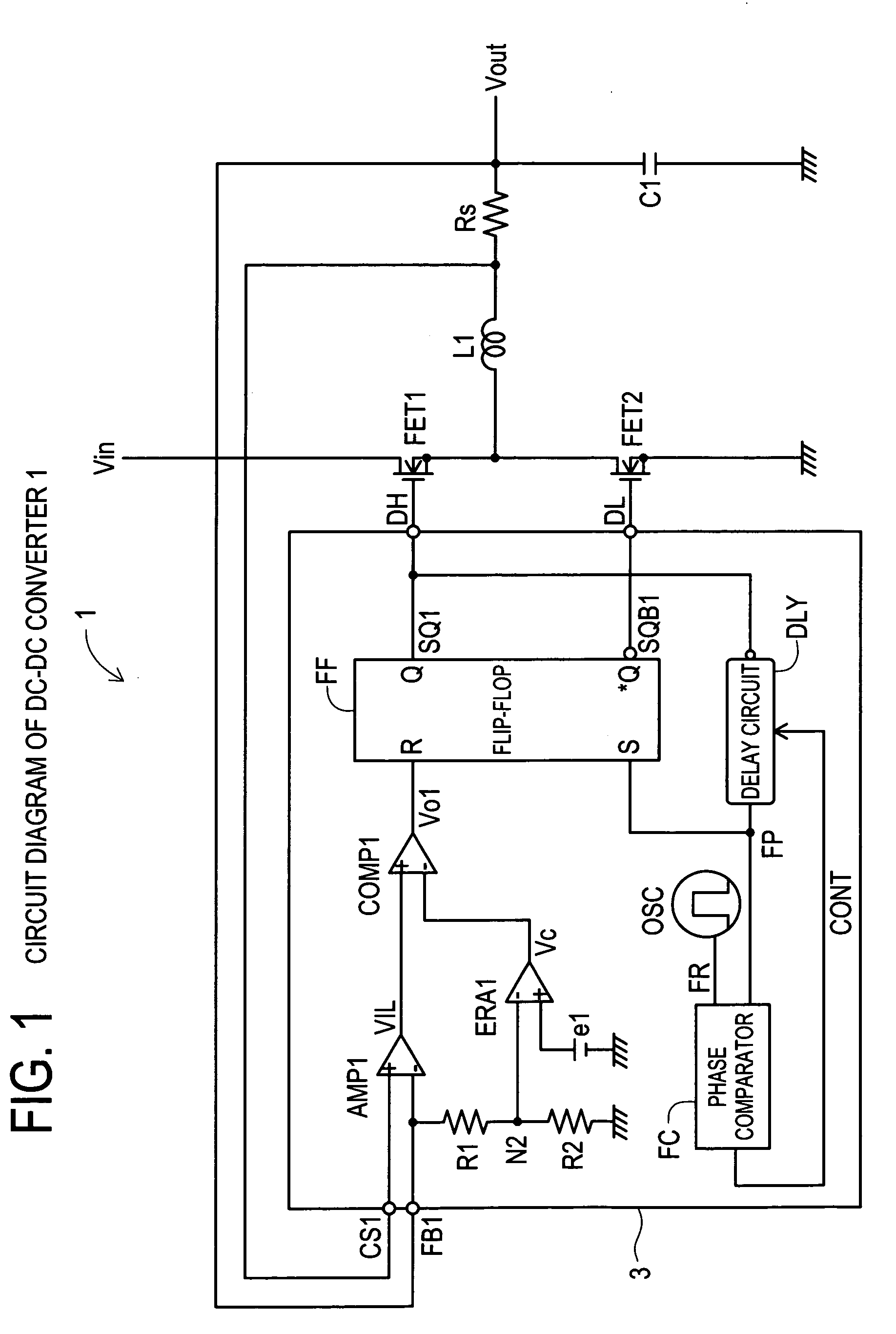
[0029]A DC—DC converter 1 according to the present invention will be explained with reference to FIG. 1. The DC—DC converter 1 includes a control section 3, a choke coil L1, a main switching transistor FET1, a synchronous rectification transistor FET2, a smoothing capacitor C1 and a current sense resistor Rs.

[0030]In FIG. 1, an input voltage Vin is connected to an input terminal of the transistor FET1, and an input terminal of the choke coil L1 is connected to an output terminal of the transistor FET1. An output voltage Vout is outputted from an output terminal of the choke coil L1. An output terminal DH of the control section 3 is connected to a control terminal of the transistor FET1. An input terminal of the transistor FET2 as a synchronous rectification switch circuit is grounded, and an output terminal thereof is connected to the input terminal of the choke coil L1. An output terminal DL of the control section 3 is connected to a control terminal of the transistor FET2. The smo...

second embodiment

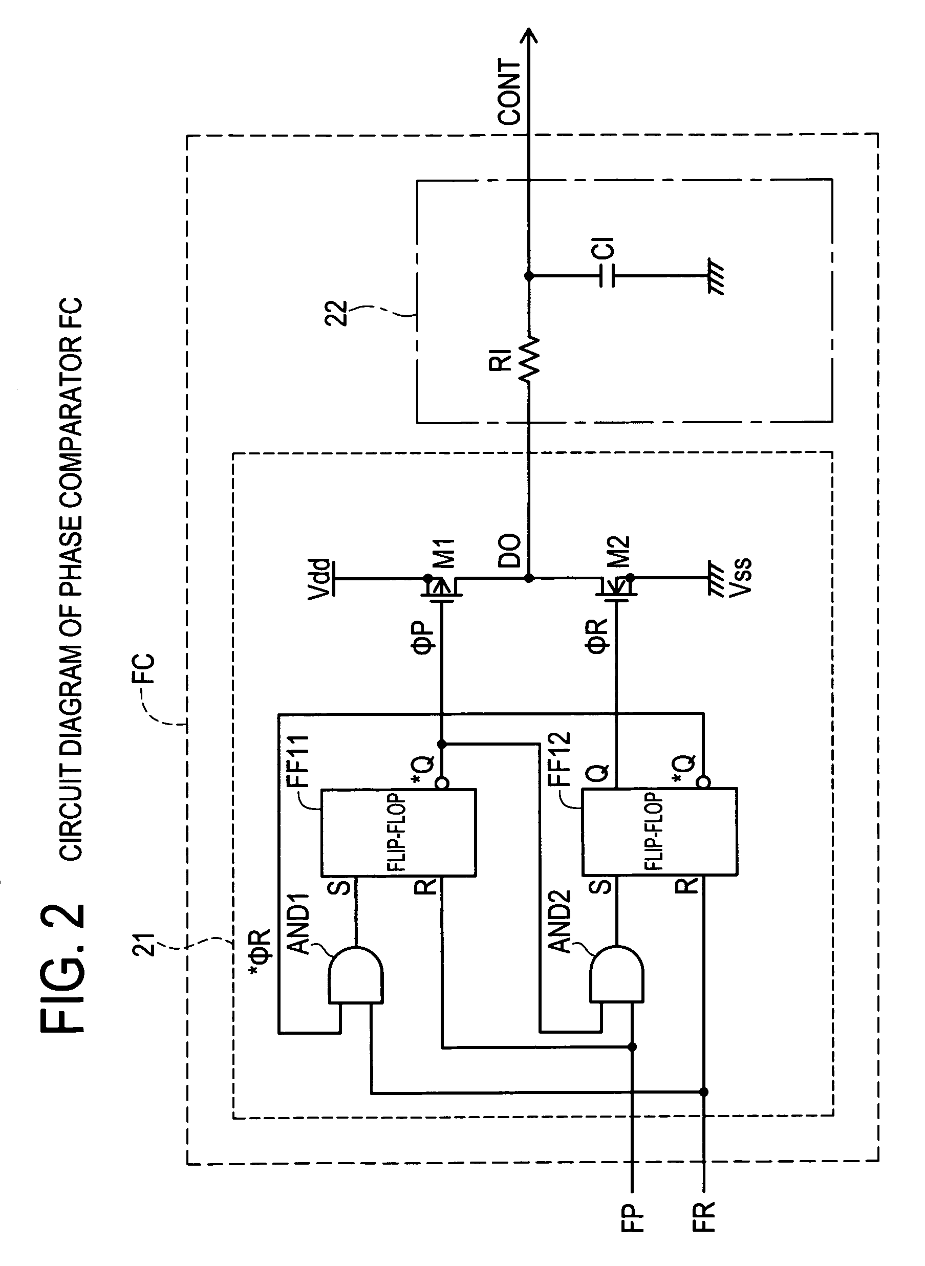
[0064]A DC—DC converter 1a according to the present invention will be explained with reference to FIG. 8. A control circuit of the DC—DC converter 1a includes a control section 3a in place of the control section 3 of the DC—DC converter 1 shown in FIG. 1. The control section 3a further includes voltage comparators COMP2 and COMP3, an AND-gate AND3 and OR-gate OR1 to the control section 3.

[0065]An output terminal of the error amplifier ERA1 is connected to the inverting input terminal of the voltage comparator COMP1 and a non-inverting input terminal of the voltage comparator COMP3. A reference voltage e3 is connected to an inverting input terminal of the voltage comparator COMP3. An output terminal of the voltage comparator COMP3 is connected to one input terminal of the AND-gate AND3, and the output terminal of the delay circuit DLY is connected to the other input terminal of the AND-gate AND3. The node N2 is connected to an inverting input terminal of the voltage comparator COMP2,...


PUM


Abstract

It is an object of the present invention to provide a control circuit and a control method for a current mode control type DC—DC converter capable of preventing a subharmonic oscillation even if an on-duty is not less than 50% and capable of preventing a switching frequency from fluctuating depending on an input voltage. When a high-level output signal Vo1 is inputted to a reset input terminal R of a flip-flop FF, a transistor FET1 is turned off. A phase comparator FC outputs a comparison result signal CONT in accordance with a phase difference between a delay signal FP and a reference signal FR. A delay circuit DLY outputs a high-level delay signal FP after the passage of a delay time DT adjusted in accordance with the comparison result signal CONT from the turn-off of the transistor FET1. The transistor FET1 is turned on in accordance with an input of the high-level delay signal FP.

Description

CROSS-REFERENCE TO RELATED APPLICATIONS[0001]This application is based upon and claims the benefit of priority from each of the prior Japanese Patent Application No. 2005-353795 filed on Dec. 7, 2005, the entire contents of which are incorporated herein by reference.BACKGROUND OF THE INVENTION[0002]1. Field of the Invention[0003]The present invention relates to a control circuit and a control method for a current mode control type DC—DC converter, more particularly, it relates to the prevention of a subharmonic oscillation occurring when an on-duty exceeds 50%.[0004]2. Description of Related Art[0005]FIG. 9 is a circuit diagram of a current mode DC—DC converter 100 of fixed off-time control. When a main switching transistor FET1 is turned on, an inductor current flowing through a choke coil L1 is increased. When the inductor current fed back via an input terminal FB1 becomes larger than an error amplification signal Vc, the transistor FET1 is turned off only for a fixed time. After ...

Claims


Application Information

Patent Timeline
IPC IPC(8): G05F1/40
CPCH02M3/1588Y02B70/1466Y02B70/10H02M3/155
Inventor HASEGAWA, MORIHITO
Owner CYPRESS SEMICON CORP
Why Eureka
Try Eureka